This thread has been locked.

If you have a related question, please click the "Ask a related question" button in the top right corner. The newly created question will be automatically linked to this question.

CSD18511KCS: Can the high side MOS maintain continuous output?

Part Number: CSD18511KCS
Other Parts Discussed in Thread: TINA-TI

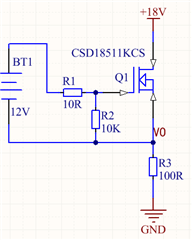
The driving method shown in Figure 1 does not require PWM for the driving signal. Can we keep HO consistently outputting high levels and LO consistently outputting low levels?

     Figure 1

Thanks

  • Liujun,

    Apologies for the delay in response due to the holiday here in the USA.

    In answer to your question, this depends on the floating supply for the HS FET.  In a bootstrap circuit usually used, the floating supply is held by a capacitor that needs off time to recharge (it’s basically a very basic version of a switched capacitor circuit).  But in the image you provided, the floating supply is undefined.  So it’s not possible to say whether the HS can be left on indefinitely.  From a FET standpoint, keeping the HS on forever and LS off forever shouldn’t be an issue.  Obviously, you need to avoid having both on at the same time to avoid shoot-through/short circuit.

    Thanks

    Chris

  • No problem at all.

    If there is no floating drive circuit, how can we ensure that HS is always conductive?

    Thank you!

  • Hello Liujun,

    Thanks again for your interest in TI FETs. In order to keep the high side FET turned on, you must apply a voltage at the gate that is at least 4.5V greater than the DC input voltage connected to the drain. When the FET is on, the drain and source voltages are approximately equal so VGS = Vgate - Vdrain and must be > 4.5V. Please note, leaving the HS on continuously will saturate the inductor which could cause excess current flow through the FET and damage it.

    Best Regards,

    John Wallace

    TI FET applications

  • Hello John,

    Thank you very much for your answer

    As shown in Figure 1, my personal understanding is that if HO keeps outputting a high level and LO keeps outputting a low level, then Q1 will remain continuously conductive

    I don't know if it's correct?

  • Hi Liujun,

    I believe you are correct but you need to make sure that the output of the opto-isolator drives the gate to at least 4.5V greater than DC voltage applied to the drain of the high side FET to ensure it remains on.

    Thanks,

    John

  • Hi,

    Can Vgd be greater than 4.5V to maintain continuous conduction of high-end FETs?

    Thank you

  • Hi Liujun,

    In general, all MOSFET datasheets specify the minimum value of VGS where Rds(on) is tested and guaranteed. This is true for all TI FETs including the CSD18511KCS datasheet which specs Rds(on) at a minimum VGS = 4.5V. As I explained in my earlier response, when the FET is on the drain and source voltages are approximately equal. For a high side switch where the source is not connected to GND, the gate voltage must be pulled up higher than the drain voltage (because Vdrain ≈ Vsource) by the minimum VGS value where Rds(on) is specified in the datasheet. The voltage can be higher (all the way up to the abs max value specified in the datasheet which is 20V for the CSD18511KCS). The FET is turned on by applying a voltage between gate and source not between gate and drain.

    Thanks,

    John

  • The voltage parameter of the battery (BT1) in Figure 2 is 12V7AH, and the drain of the MOS transistor is 18V. 18V and the battery are two different independent power sources. Is the MOS transistor conducting? What is the voltage of VO?

           Figure 2

    Thank you

  • Hi Liujun,

    In your circuit diagram the FET will be operating in the saturation region (Vds > Vgs - Vth). This is also known as linear mode operation. I created the attached simple TINA-TI simulation to estimate the DC operating conditions for your circuit. With a typical device, VO = 9.82V, VGS = 2.18V, VDS = 8.18V and ID = 98mA. In order to guarantee that the FET is on, VGS must be at least 4.5V. If the battery voltage is say 23V, then the FET will be fully turned on: VO = 18V, VGS = 5V, VDS = 498μV and ID = 179.5mA.

    Best Regards,

    John

    CSD18511KCS_Bias.TSC

  • This morning, I conducted an experiment according to Figure 1, where the BT1 voltage is 12V and the VO output is 18V. If 18V is replaced with DC700V, will the VO output be 700V? Will this 700V voltage affect or damage the battery?

     The schematic of the CSD18511KCS_ Bias.TSC file does not match Figure 1. Can we simulate it according to Figure 1?

    Thank you!

  • Hi Liujun,

    The CSD18511KCS has a absolute maximum VDS rating of 40V. You cannot apply 700V to the drain of the FET. It will be destroyed and likely will expose the battery to 700V causing catastrophic failure. You will need a FET with a breakdown voltage > 700V.

    Thanks,

    John

  • Hi John Wallace1,

    Sorry! Will the IGBT in Figure 3 conduct? What is the voltage output by VO if IGBT is conducting? Will DC700V cause damage to the battery?

    Thank you!

                  Figure 3

  • Hi Liujun,

    An IGBT is similar to a MOSFET. The gate-emitter voltage must be driven to a high enough voltage to minimize the collector-emitter voltage. In the circuit diagram, the battery is referenced to the emitter terminal and VGE should be approximately 12V. I pulled up the datasheet for the IGBT in the diagram and it specifies VCE(sat) at VGE =15V. Looking at Figure 1 in the datasheet, it looks like VCE(sat) will be somewhat higher with VGE = 12V. The battery should not be damaged with 700V at the collector. I would recommend contacting the IGBT vendor for more detailed technical assistance as TI does not make IGBTs.

    Thanks,

    John

  • Hi John Wallace1,

    Thank you for your answer