A related question is a question created from another question. When the related question is created, it will be automatically linked to the original question.
If you have a related question, please click the "Ask a related question" button in the top right corner. The newly created question will be automatically linked to this question.
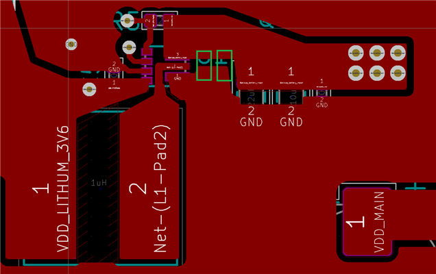
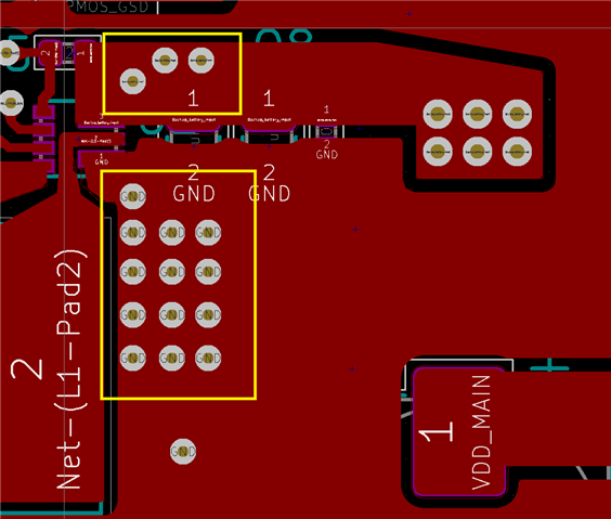
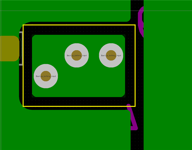
1.The placement of output capacitor is the most important thing for Boost converter, please place the output capacitors as much as close to VOUT / GND pin of IC. (as shown in the green square). Otherwise, there may be a risk of damage when operating at large load current.
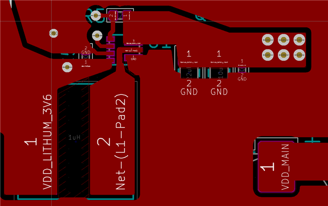
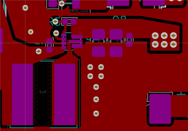
2.About the vias, they are used to improve the thermal performance, if the IC is operating at large current for a long time, we recommend to add vias, otherwise the temperature may be very high, and hit thermal shutdown early.