This thread has been locked.

If you have a related question, please click the "Ask a related question" button in the top right corner. The newly created question will be automatically linked to this question.

TPS6521905: LDO combine and programing quesion

Part Number: TPS6521905


Dear Team,

i have some questions regarding TPS6521905 PMIC.

1) if i understand correctly if the PMIC NVM is not programed all BUCK and LDO outputs are off?

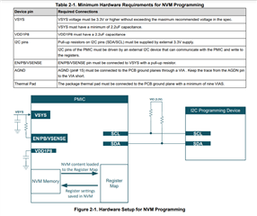
1a) if we want to do in-circuit NVM programming once the PMIC is soldered to our PCB , is it possible and what signals do we need to provide from outside to do this? 

2) Is it possible to tie the LDO1 and LDO2 output together if they have same output voltage to support 800mA ?

3) if BUCK1 or BUCK2/3 is not used what is the proper way to terminate it  from HW and SW side?

4) if LDO3 and LDO4 are not used what is the proper way to terminate it  from HW and SW side?

Best Regards,

d.

  • Hi d,

    1. You are correct, for the TPS6521905 PMIC version all BUCKs and LDOs are disabled by default.
      1. In circuit programming is possible with the minimum hardware configurations shown below (From Figure 2-1 in TPS65219 Non-Volatile Memory (NVM) Programming Guide)

    2. As far as I know this device does not support parallel LDO configurations.

    3. For unused BUCKs, you may leave the LX pins floating, connect the PVIN pins to VSYS (no input cap needed), and connect FBx pin to GND

    4. For unused LDOs, you may leave VOUTx pin floating and connect PVIN pins to VSYS (no input cap needed).

    Regards,

    James