This thread has been locked.

If you have a related question, please click the "Ask a related question" button in the top right corner. The newly created question will be automatically linked to this question.

[FAQ] UCC5880-Q1: Getting Started with UCC5880-Q1 Without SPI

Part Number: UCC5880-Q1

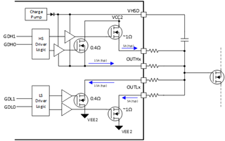
How and Why to use UCC5880-Q1 without SPI

  • Getting Started with UCC5880-Q1 Without SPI

     The UCC5880-Q1 device is an isolated, highly configurable adjustable slew rate gate driver. One element that makes UCC5880 very useful in high power EV/HEV applications is it’s SPI based device configurability, verification, and diagnostics.

    Although the SPI communication provides a lot of flexibility for the system, some applications do not require the complexity of SPI. Customers who are not familiar with SPI may appreciate its benefits, but when getting started with this new driver, may want to do a simple evaluation without spending time and resources developing the software. The UCC5880-Q1 device can support this as it can be used without SPI communication for initial evaluation of the device

    Using this functionality, the engineer can evaluate basic driver performance like drive strength, switching losses with power modules, adjustable gate drive, short circuit protection, etc. The user will be able to speed up the evaluation process since there is no requirement to develop any new code or even connect to a computer.


    How to configure the SPI pins when not used?

    Using the driver without SPI connection requires certain configurations to the SPI pin functions. Leaving input pins floating can cause faults from noise coupling into them. Output pins can be left floating. These changes are listed below.

    Pin Name

    Configuration

    SCLK

    Tie to GND1 when not used

    nCS

    Tie to VCC1 when not used

    SDI

    Tie to GND1 when not used

    SDO

    Can be left open

    Table 1: Pin Name and Configuration


    How to change the Drive Strength without SPI?

    The adjustable drive feature of UC5880-Q1 allows the drive strength to be set to 1 of 3 different drive strengths on the fly. The device has a split output structure: OUTH1, OUTH2, OUTL1, and OUTL2. OUTH1 and OUTL1 have a 15A drive strength, while OUTH2 and OUTL2 have a 5A drive strength. The Output structure is shown in the diagram below.


                                                                                            Figure 1: UCC5880-Q1 Output Structure

    This is to control the turn on/off of the FET for different system conditions to optimize the tradeoff between switching energy loss and Drain to Source Overshoot. UCC5880-Q1 has 3 GDx pins (GD0, GD1, GD2) on the low voltage to enable use of this function without the need for SPI. Changing the gate drive strength without SPI is fairly simple. These combinations are listed below and also listed in the datasheet.

    GD2

    GD1

    GD0

    Function

    0

    0

    0

    Controlled by SPI registers

    0

    0

    1

    OUTL1 + OUTH2

    0

    1

    0

    OUTL2 + OUTH1

    0

    1

    1

    OUTL1 + OUTH1

    1

    0

    0

    OUTL2 + OUTH12

    1

    0

    1

    OUTL12 + OUTH2

    1

    1

    0

    OUTL12 + OUTH12

    1

    1

    1

    OUTL2 pull low, Fault Reset

    Table 2: GDx Pin Truth Table


    What are the main challenges when not using SPI?

    There are three main challenges when not using the SPI functionality. First is the reconfiguration of the device. SPI allows the user to configure the configuration registers and action register. When not using the SPI, the configurations and actions will be the default programmed values listed in the datasheet.

    Second is the live monitoring ability of the device. The device has an internal 10-bit ADC and two analog inputs (AI1 and AI2) which are used to read and monitor useful measurements such as, DC-Link voltage, gate threshold, internal die temp, current sense, etc. The ADC also has DESAT(CS), VCC2, Gate voltage threshold and junction temperature measurement options. Without SPI, the user will have to implement other methods for all of these measurements.

    Last but not least is the fault supervision. The UCC5880-Q1 device has 1 status and 2 fault registers with over 30 fault and warning Classifications. Additionally, there are also commanded BIST diagnostics available for the PWM Lane (INP to output), Shoot Through Protection, Gate Voltage Monitoring, Gate Drive Strength Monitoring, DESAT comparator, SC comparator, OC comparator, Clock Monitoring, Configuration CRC, and Digital Comparators. Without SPI it will be challenging to understand what fault has occurred in the system. When a fault occurs, either or both of the nFLT pins will pull low. Holding all the 3 GDx pins high will reset the fault, but there is no way to read exactly what fault has occurred. The best way to address this is to make the sure the default register settings exactly match the requirements of the application and then probe these points to make sure the device is operating as it should. The next section discusses commonly seen faults on our EVM when not using SPI and how to solve them.


    What are the common Problems and Fixes?

    As said previously, when using the UCC5880-Q1 device without SPI it will be challenging to diagnose the cause of any faults once the nFLT pins pull low. Below are some basic common issues that are easily diagnosable when using the device without the SPI fault reporting. The UCC5880-Q1 EVM provides the easiest solution to evaluate the device with and without SPI. Test points are provided for each signal to diagnose any faults.

    Problem

    Evaluation

    Explanation

    Corrective Action(s)

    No PWM output (no fault reported)

    Check Status of GDx pins

    Setting all GDx pins to all 0s give control to the SPI registers, which is weak drive strength by default


    Setting GDx to all 1s pull the output low and reset the faults

    Set the GDx pins to a combination that provides an output

    No PWM output and nFLT1 reported (STP or SC/DESAT fault)

    Check the interlock settings

    If PWM is high for both high side and low side drivers, STP fault will occur

    Remove the interlock connections and clear the fault by pulling all GDx pins high, or add deadtime to input signals

    Check SC/DESAT status

    DESAT is triggering and causing output to pull low

    The DESAT protection must be disabled when not connected to a FET module by tying the desat pin to GND

    nFLT 1 and nFLT 2 reported on startup (BIST fault)

    BIST failure

    The device will automatically run diagnostics on all UV/OV comparators and report fault if the spec is not met

    Power cycle and set all power supplies correctly


    nFLT1 and nFLT2 reported on startup or during switching (VREF, VCCREG, VCC1UV/OV, VCC2UV/OV fault)

    Check power supply values

    Power supplies not high or low enough/ dip or spike in power supplies

    Set the power supply values to meet the default configuration values

    No PWM during Short Circuit Test (DT or STP fault)

    Check the interlock settings

    STP protection prevents shoot through

    Remove the interlock connections

    Check DT settings in the function generator

    Dead time is enforced and prevents short circuit

    Remove DT, the driver has no DT by default

    Table 3: Common Problems and Fixes


    What are the default Settings?

    Since the device can only operate with the default configurations, it is important to understand if all the default settings align with the evaluation needs. The default settings are in table 4, 5 and 6. The default configurations are also located in the Datasheet under the Register map section.


    Table 4: Configure Registers Default Values

    Register Type

    Bit Name

    DFLT Value

    Config 1

    UVLO1_TH

    2.45V


    OVLO1_TH

    5.65V


    NFLT2_MUX

    nFLT2


    TDEAD

    No Deadtime


    IO_DG

    No Deglitch


    RESET_MUTE_EN

    Enabled

    Config 2

    MCLP_TH

    2V


    UVLO2_TH

    9V


    OVLO2_TH

    22V


    UVLO3_TH

    -2V


    OVLO3_TH

    -8V


    GM_BLK

    4052ns


    OC_EN

    Disabled


    DESAT_SC_SEL

    DESAT Enabled


    MCLP_EN

    MCLP Enabled

    Config 3

    SC_BLK

    87ns


    OC_TH

    0.25V


    DESAT_SC_DG_EN

    Disabled


    DESAT_SC_TH

    10V


    DESAT_ICHG

    0.5mA


    STO_2STO_CURR

    300mA


    VGTH_MEAS_EN

    Disabled

    Config 4

    2STO_TIME

    122ns


    MCLP_EXT_EN

    Internal


    VCE_CLMP_HLD_TIME

    100ns


    2STO_STO_SEL

    STO


    VCECLP_EN

    Enabled


    IZTC_EN

    Disabled


    DOUT_FREQ

    13.9kHz


    DOUT_CH_SEL

    Disabled

    Config 5

    ADC_SAMP_MODE

    Disabled


    ADC_SAMP_DLY

    280ns


    ADC_ON_DESAT_SEL

    Disabled


    ADC_ON_VCC2_SEL

    Disabled


    ADC_ON_TEMP_SEL

    Disabled


    ADC_ON_CH2_SEL

    Disabled


    ADC_ON_CH1_SEL

    Disabled


    ADC_OFF_VCC2_SEL

    Disabled


    ADC_OFF_TEMP_SEL

    Disabled


    ADC_OFF_CH2_SEL

    Disabled


    ADC_OFF_CH1_SEL

    Disabled


    IZTC_SEL

    100uA


    ADC_SAMP_DLY_MULT

    x1

    Config 6

    ADC_EDGE_MODE_SEL

    Continuous


    OC_BLK

    490ns


    Table 5: Action, Digicomp, ADC, STATUS & FAULT Registers Default Values

    Register Type

    Bit Name

    DFLT Value

    ACT 1

    OVLO1_ACT

    STATUS+nFLT1+OUTL* pull low


    UVLO1_ACT

    STATUS+nFLT1+OUTL* pull low


    OVLO2_ACT

    Disabled


    UVLO2_ACT

    STATUS+nFLT1+OUTL* pull low


    OVUV3_ACT

    Disabled


    ADC_ACT

    STATUS+nFLT2


    SPI_ACT

    STATUS+nFLT2


    CFG_CRC_ACT

    STATUS+nFLT2

    ACT 2

    INT_REG_ACT

    STATUS+nFLT1+OUTL* pull low


    TRIM_CRC_ACT

    STATUS+nFLT1+OUTL* pull low


    GD_TWN_ACT

    STATUS+nFLT2


    CLK_MON_ACT

    STATUS+nFLT1+OUTL* pull low


    OC_ACT

    FAULT+nFLT1


    VCECLP_ACT

    FAULT


    STP_ACT

    STATUS+nFLT1+OUTL* pull low


    PWM_LANE_ACT

    STATUS+nFLT1+OUTL* pull low


    INT_COMM_ACT

    STATUS+nFLT1+OUTL* pull low


    SC_DESAT_ACT

    STATUS+nFLT1+OUTL* pull low

    Act 3

    GM_GD_ACT

    FAULT+nFLT1+OUT*high impedance

    DIGICOMP 1

    THRESH_AI1

    Top 8 bits of ADCDATA1


    DCOMP1_EN

    Disabled


    DCOMP1_DIR

    DCOMP1_FAULT high when ADCDATA1<THRESH_AI1


    DCOMP1_ACT

    Disabled


    DCOMP1_DEGLITCH

    2 comparison before fault occurs

    DIGICOMP 2

    THRESH_AI2

    Top 8 bits of ADCDATA2


    DCOMP2_EN

    Disabled


    DCOMP2_DIR

    DCOMP1_FAULT high when ADCDATA2<THRESH_AI2


    DCOMP2_ACT

    Disabled


    DCOMP2_DEGLITCH

    2 comparison before fault occurs

    ADC 1-6

    All Bits

    Holds ADCDATA from last AI measurement

    Status

    All Bits

    Indicated STATUS register of the device

    Fault 1

    All Bits

    No Faults

    Fault 2

    All Bits

    No Faults


    Table 6: Control Registers Default Values

    Register Type

    Bit Name

    DFLT Value

    Control 1

    CLR_FAULT

    No action


    GATE_OFF_CHK

    No


    GATE_ON_CHK

    No


    OC_CHK

    No


    DESAT_CHK

    No


    SC_CHK

    No


    GD_READ_EN

    No


    CLK_MON_SEC_CHK

    No


    CLK_MON_PRI_CHK

    No


    CFG_CRC_CHK

    No


    DCOMP1_CHK

    No


    DCOMP2_CHK

    No


    CLR_SPI_CRC

    No


    PWM_LANE_CHK

    No


    STP_CHK

    No


    GD_FAULT_CHK

    No

    Control 2

    OUTH_SEL

    OUTH2 only


    OUTL_SEL

    OUTL2 only


    ASC_STRENGTH

    OUTL2/OUTH2 only


    CURPROT_ASC_EN

    Enabled


    AI2_PUPD

    Pull Up/Down Disabled


    ASC_LEV_SEL

    Follows AI2()ASC_SEC


    ASC_DELAY_SEL

    2.3us


    ASC_EN_HIZ_EN

    ASC Low - Output low

    Control 3

    SPITEST

    0


    Should I use the UCC5880-Q1 in my final design without SPI?

    Although the non-SPI functionality of UCC5880-Q1 is a great tool to evaluate the gate driver, it is not recommended to be used for the final design. The fault reporting, monitoring and configurability options are too valuable to not be taken advantage of. The inability to diagnose faults will add many challenges to the system design and make it difficult to even enable the use of some basic safety functions of the final system.

    The design of an SPI based software for gate driver control can be intimidating for new users, but TI has a solution to ease the complexity of creating this code with our Complex Device Driver (CDD). the goal of the CDD is to develop a modular, platform independent, configurable SPI interface [support different modes] in complying with the ASPICE process. The CDD is developed on the MCU AM26x platform, to handle SPI Interface, low voltage IO pins (FLT, PWM, Primary ASC, DOUT), diagnostics, FLT monitoring and to read ADC data. The CDD can be integrated to the customer’s different microcontroller AUTOSAR & non AUTOSAR stack using the integration guide and the CDD configuration files. More information can be found in the UCC5880-Q1 product folder.