A related question is a question created from another question. When the related question is created, it will be automatically linked to the original question.
If you have a related question, please click the "Ask a related question" button in the top right corner. The newly created question will be automatically linked to this question.
TPS23752: TPS23752 POWER OVER ETHERNET, OUR LAN8740 IC heating very much.
Hi Diang, any suggestion I have messure current on 12V-P. There is a very much fluctuation in current from 108mA to 280mA approx. Please advise me any suggestions.
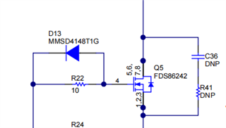
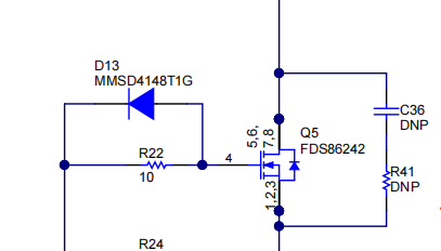
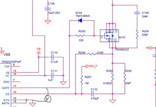
1. D13 ensure a fast switching off speed for Q5. This can help to reduce the switching off energy. If you have a secondary side sync FET, this also help to reduce the pri-sec FETs shoot-though time.
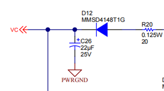
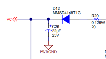
2.There should be no issue to swap D12 and R20 position.
3. The 12V-P voltage has 1.68-V peak-peak ripples. Just wondering if you have a LDO to transformer 12V-P to to 3.3-V input to source LAN8740A. Normally LDO should alleviate most of the ripples.
4. For the output ripple, looks VC is higher than the UVLO and VDD is stable too. Could you help measure the GATE-RTN voltage? Just wondering if the GATE is discontinuous that causes large ripples on 12V-P.
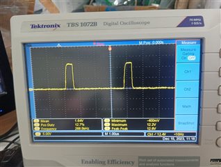
Thanks for the gate voltage waveforms. The duty cycle (D) is about 17%. And the turns ratio is 2:1.
By N*Vout = D/(1-D) * Vin, Vin is ~117V, which is higher than the 54V-POE input. Looks like the gate duty cycle could be varying at the same load current or the load is too light. Could you help to check:
- a zoom-out gate waveforms to see if the duty cycle is keeping at ~17% or it is variable at the same load current
- if the Vout could be stable when you have a heavier load.
I have attached photo for Gate waveform when load as only our device, vary duty cycle 12% - 16%
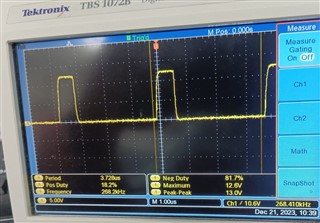
I have attached photo for Gate waveform when load as only our device + Lock, vary duty cycle 17% - 18%.
In Somedevices get back from field, which has issue regarding Vc pin damage (It show continuity, or it show low impedance).
We check waveform in which we find ripples approx. 1.2V peak to peak, right now we reduce peak to peak voltage up to 440mV to 600mV with added 4.7uF-50V capacitor at Vc pin.
Also, we reduce output voltage 12V-P ripples up to 280mV with added 47uF-50V Ceramic capacitor.
What more protection we need to take care for this issue. will it help when we added 12V Zener at Vc pin?
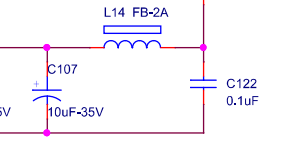
I saw you add a CLC pi-filter before Vout, and I am wondering if you could increase the inductor inductance meanwhile keep it not saturated. It may further helps to reduce the Vout ripple.
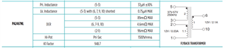
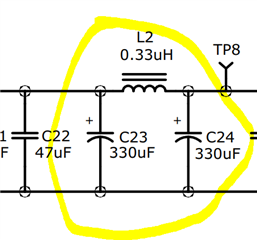
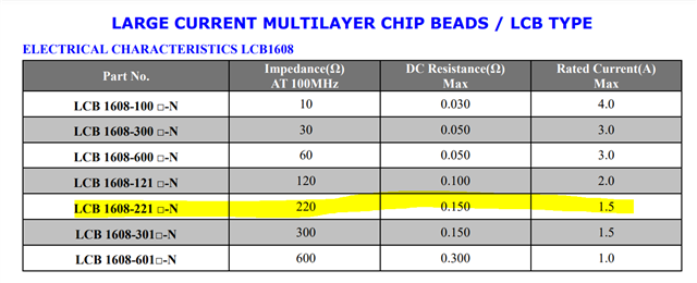
LCB1608-221Y-N is rated for 1.5A. I am wondering what is your output power at 12-V. Looks like P needs to be smaller than 18W.
Using 2*pi*100e6*L=220, L is ~0.35 uH at 100MHz. You can try to further increase the inductance to 2.2 - 4.7 uH which may help to flat the current and the voltage ripples.
With the holidays here, many device experts are currently out of the office. When they return they will look into this and provide a response. Please expect some delay accordingly.
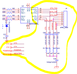
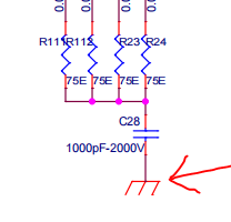
In our design we use plastic Cat5 Jack for POE connections. Is it correct circuit, which is I have sent earlier (we connect Earth ground, but we use plastic Cat5 Jack), or we need to change GND at Bob-Smith terminations?
For the inductance value in PI-filter, normally a large inductance of the inductor and a small stray inductance in the capacitors can make the performance better. BLM18SG121TN1D is a 0603 packaged one and it may not be large enough. You can use the following link to help design a filer: www.ti.com/.../SSZT824
In our design we use plastic Cat5 Jack for POE connections. Is it correct circuit, which is I have sent earlier (we connect Earth ground, but we use plastic Cat5 Jack), or we need to change GND at Bob-Smith terminations?
We did see some products make the Bob-Smith termination ground floating when a plastic RJ45 is used. It may depend on the product application, and looks like floating is optional.
This is more related to EMI and I do not think it has big impact for heating.