This thread has been locked.

If you have a related question, please click the "Ask a related question" button in the top right corner. The newly created question will be automatically linked to this question.

MC33063A: Vin range under IBB design

Part Number: MC33063A
Other Parts Discussed in Thread: MC34063A

Hi Team

Nice to link up.

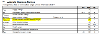
I have a quick question about MC33063A inverting design, is Vin range still 3~40V under inverting voltage output.

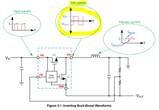
Due to under buck inverting output design, VIN+|VOUT|<VINMAX, but due to MC33063A basic likes buck-boost, so does that means Vin could up to 40V?

Thanks a lot

Irene

  • Hi Irene,

    Thanks for using the e2e forum for this question.

    You are correct that there are special conditions when operating MC33063A with negative output voltage.
    The datasheet says there is a abs max voltage from collector to emitter of 40V (Vce).
    Looking at the block diagram, we see that the collector is connected to VIN and the emitter to the switch note (SW).
    During off time of the switch, the SW voltage drops to the negative output voltage.
    For example, at Vin 35V, Vout -10V, the Vce voltage would be 35V - (-10V) = 45V. This would be out of spec.

    To support negative output voltages, your equation is correct VIN+|VOUT|<VINMAX 

    Best regards,
    Niklas

  • Thanks Niklas for your quick reply.

    According to this appnote, I thought only buck designed IBB has limit like  VIN+|VOUT|<VINMAX , but buck-boost designed IBB doesn't has this kind of limitation. So in that case my understanding is wrong, any IBB both has  VIN+|VOUT|<VINMAX  this VIN limitation, right?

    1273.Working With Inverting Buck-Boost Converters.pdf

    irene

  • Hi Irene,

    Your understanding regarding the VIN limitation is correct.
    However, I am referring to the switch note limitation of an IBB.

    Therefore, the equation I am looking at is VIN+|VOUT|<SW MAX
    This limitation is 40V as well for MC34063A.

    Best regards,
    Niklas

  • Hi Niklas

    Thanks for your explanation.

    Another question is about "non-Darlington configuration" .According to datasheet, non-Darlington configuration should be like Figure 5 b), which has a resistor R* between and pin1.Here are the questins:

    1. where is the R* connected with inductor?

    2. The notes said when Vin is constant, R* is 0ohm ,which means the non-Darlington configuration is exactly same with Darlington configuration ?

    irene

  • Hello Irene,

    The non-Darlington variant is a concept where the base-emitter voltage of the external transistor is higher than the collector-emitter voltage which will bring that external transistor into hard saturation.
    To do that you will need a special inductor which allows access "somewhere in the middle". The question is where.
    In addition, you would probably need a lot of experiments to find out the value of R'.

    I do not know of any customer who is actually using this concept.

    Best regards
    Harry