This thread has been locked.

If you have a related question, please click the "Ask a related question" button in the top right corner. The newly created question will be automatically linked to this question.

TPS27S100: OUTPUT GO HIGH IF YOU CONNECT ONLY VDD TO GND

Part Number: TPS27S100

Hello,

I have a problem with TPS27S100 partnumber.

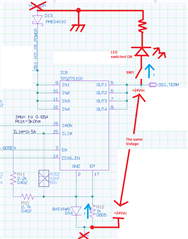
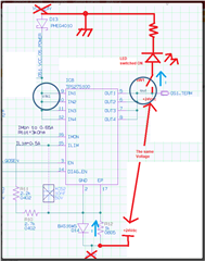
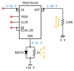
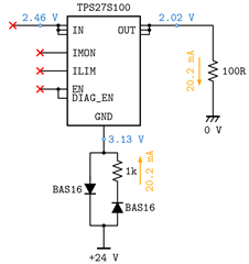
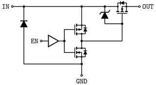
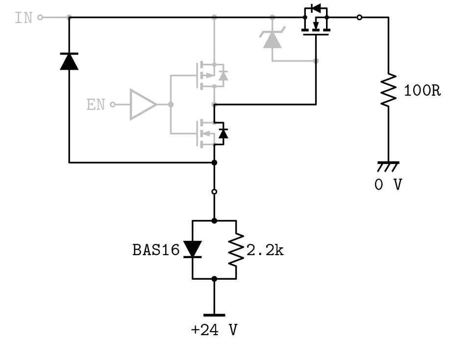
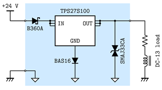
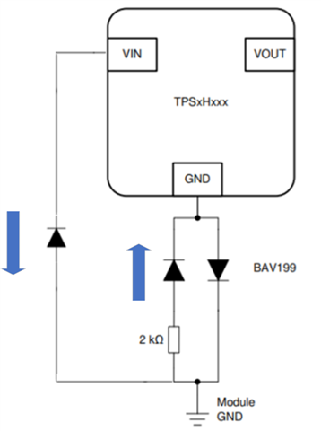
I report the test in this schematics:

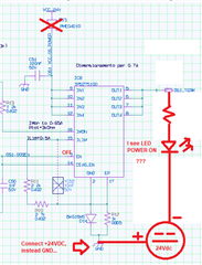
When I connect only +24Vdc to GND Network, the output go HIGH and i see led power on.

This always happens even if I don't activate the EN pin (pin 3).

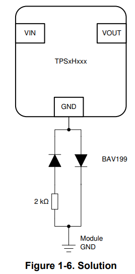
If i remove R12 the output is LOW, but in this case i loose the reverse current protection in case of inductive load.

Can you help me?

Many thanks.

Best regard.

  • Hello, 

    A conventional reverse polarity has ground on the supply and power to the ground. 

    Can you please explain the test here and why ground in on the output? 

    It appears you are triggering a double fault scenario where there is a loss of ground and a low impedance short from VS to board ground

    Do note, there is a known parasitic path in the device further detailed in this app note:

    https://www.ti.com/lit/an/slvaes9a/slvaes9a.pdf?ts=1701985514360&ref_url=https%253A%252F%252Fwww.google.com%252F

    If this double fault scenario is something you expect to see, you will have to switch up your ground network to something similar to below: 

    Best Regards, 

    Elizabeth 

  • Hi Elizabeth,

    Thank for you reply, but the problem is not resolved.

    If I reverse the polarity, the problem is the same. The output is always HIGH. 

    The reverse of polarity, in my opinion, is a single fault NOT double fault. 

    This is the schematic:

    The reason of this test that the certification body carries out a polarity reversal test of the device and checks whether the outputs are low.

    The low impedance short circuit you are talking about does not exist because there is a Diode D13 at the input of the VIN of the SmartFET.

    If switch SW1 is open and i power on the MOS in reverse polarity, I find in the OUTPUT +24Vdc and if I switch on SW1 the led light up.

    For 200-kΩ internal parasitic path that you are talking, from the ground pin to the output pin, as specified at this table:

    I should se see this circuit:

    Assuming I have a load of 0 ohm and ignoring the drop on the internal diode, I should see a maximum current of I=24/201kOhm = 0.119 mA.

    However I saw that the current only depends on the output load.

    Other information I can give you is that I see in the VIN PIN is 23.32Vdc and EN 23.45Vdc (pin 3).

    The only solution in my opinion, is remove R12 however, as I said, but i  loose the reverse current protection in case of inductive load.

    I have used power devices in the past and have never had this problem.

    Can you give me more information?

    Many thanks.

    Ivan

  • Hello,

    Please can you reply me?

    Many thanks.

    Ivan

  • Hi Ivan, 

    Apologies for the delay during the holidays! 

    Thank you for providing that information! I have a few questions which will help us determine the root cause which reference the schematic below: 

    1. Please probe IN1; Is this node at 24V? 
    2. What output loads have you tested and what is the current being pulled specifically by the output (circled below)
      1. Specifically, please test under a 100ohm load; do you see 240mA pulled by the output or 24mA under a 100ohm load? 
    3. Have you tested the proposed BAV199 solution? 

    If you are seeing 24V at Vin1 and 240mA under a 100ohm load, then my suspicion is there is an external parasitic path from ground to VIN which is causing the gate to charge and the FET to conduct as noted in the provided app note. 

    If so, my recommendation would be to use the BAV199 solution as shown below in order to create a 1V difference between the supply voltage seen at the input and device ground further described in https://www.ti.com/lit/an/slvaes9a/slvaes9a.pdf?ts=1701985514360&ref_url=https%253A%252F%252Fwww.google.com%252F

    Do note, if a GND network is used, a input diode is not needed. Is there a reason an input diode is included along with a ground network in your design? 

    Best Regards, 

    Elizabeth 

  • Hello Elizabeth,


    I have a similar problem to Ivan's and I do not understand how the proposed solutions would help.


    I tested the TPS27S100 on its own, all pins are disconnected except for GND and OUT, as shown in the following schematic:

    Voltages are reported in blue, while calculated currents are shown in orange.

    The use case is not a double fault, since the 100 ohm load would be external to the circuit, connected by the end user. If they connect the power supply wrong, i. e. power supply +24 V on the circuit GND, the output activates.

    The solution with a second diode in the ground path cannot work, as the use case is very different from the one described in the SLVAES9A application note you cited. In fact, these are voltages and currents with such solution:

    In my opinion, the problem could be due to the gate driver of the output MOS. Let's hypothesize an internal structure similar to the following:

    The current finds its path through the body diode of the low-side MOS in the driver, charging the output MOS gate-source capacitance beyond the threshold voltage. Therefore, the output MOS gets activated and can conduct current coming from the protection diode at IN-GND.

    In fact, there is about 0.7 V diode drop between GND and IN.

    The only option I see to retain both inductive load protection and reverse polarity protection is to remove the resistor in the ground network and use a TVS to suppress the inductive voltage spike at the output.

    Can you please confirm this is true?

    ***

    Do note, if a GND network is used, a input diode is not needed. Is there a reason an input diode is included along with a ground network in your design?

    An input diode prevents a powered-off product from being powered from the output through the MOS body diode. The ground network cannot prevent that.

    ***

    Thank you in advance.

    Best regards,

    Federico

  • Hi Elizabeth,

    Thank to Federico that he described my same problem perfectly.

    Now Elizabeth we need urgent answers, because my project is blocked due to this problem.

    If the component has some weakness in this sense that cannot be resolved, I kindly ask you to say so and propose a possible alternative part number with similar characteristics.

    Now we wait urgent answers to Federico's questions and mine.

    Thank you.

    Best regards,

    Ivan

  • Hi Ivan, Federico, 

    Thank you for providing that information! Since the input is not at 24V, I suspect the input is being charged by the ground across the ESD diode, hence the ~0.7V drop from GND to IN as you have shown, which is partially turning on the device. 

    To confirm, could you capture results using a 2kohm resistor rather than a 1kohm resistor on the GND network? 

    To help identify a solution, Is there an amount of voltage on the output which is acceptable for your application?

    Best Regards, 

    Elizabeth  


  • Hi Elizabeth,

    these are the results with a 2.2 kΩ resistor on the GND network:

    It is pretty much clear that the equivalent circuit during the fault condition is similar to the following, assuming a simple gate driver without protections:

    In this case, neglecting the on resistance of the MOSFET (which is probably not fully turned on), the calculated current on the output is

    I = (24 V – 0.7 V) / (2.2 kΩ + 100 Ω) = 10.1 mA

    which accurately predicts what I measure, as I highlighted in my first post.


    Is there an amount of voltage on the output which is acceptable for your application?

    No. There are a number of different ways the customer can use the output of the product, including reading it as a digital value (high impedance) or connecting it to small loads, such as a LED indicator.

    Therefore,

    • in the first case, the load resistance is medium-high, hence current is very low and voltage MIGHT have a "safe" threshold which depends on digital levels in the application of the customer, which I cannot assume.
    • in the second case, similarly to the 100 Ω example, the load resistance is low and current activates the load while voltage across it remains low.

    The only safe way to implement my functionality is to remove the unwanted path.


    How can I solve the problem, considering there are tight space constraints that cause difficulties using similar (but bigger) products not showing the issue?

    Thank you.

    Best regards,

    Federico

  • Hi Federico, 

    I did some brainstorming and have an idea for us to try! 

    Essentially our root issue is when the GND of the device and the supply of the device are between 0.5V and 1V difference there is potential for unintended turn on of the FET. This can arise two ways: 

    • When VIN is floating, the internal ESD diode provides the path of least resistance to power VIN through the GND pin which forces VIN and GND to be within the 0.5-1V range. 
    • When VIN is not floating, the 200kohm resistive path described in the app note I provided creates the path to force GND within a 0.5-1V range of the supply VIN 

    A potential fix to ensure VIN is not floating is to shunt the supply to module GND by way of a diode. A good option would be a TVS or Schottky diode. A TVS diode would have the additional benefit of transient suppression in the case of a input voltage surge. 

    The BAV199 solution would still be needed to ensure the VIN to GND difference is greater than 1V during this condition. 

  • Hi Federico, Ivan, 

    Any update or questions with regard to my proposed solution? 

    Best Regards, 

    Elizabeth 

  • Hi Elizabeth,

    thank you very much for your response and sorry for the delay.

    I tried your solution by bodge-wiring components in my existing design, and it seems to work.

    However, I prefer to do further checks before confirming the answer. Currently I'm waiting for additional components from a distributor to do some more tests; I'll let you know the results as soon as possible.

    Thank you again for your patience.

    Best Regards,

    Federico

  • Hi Federico, 

    Great to hear of the positive initial results! 

    Yes please let me know the results of your further checks. 

    Best Regards, 

    Elizabeth 

  • Hi Elizabeth,

    I discussed with my manager the results obtained with your solution. It surely helps keeping the MOS in a nearly-off state (better than before), but sadly it is not enough for our application; in fact, the equivalent channel resistance we estimated in the fault condition is about 120 kΩ.

    If a customer connects the product to a high impedance interface, they might see a high logic level depending on their application and this is not acceptable.


    Instead, I propose a different solution which I'm testing by driving a DC-13 load (by standard IEC 60947-5):

    Our product is highlighted in blue, connections done by the customer are external. With this solution:

    1. the product is protected by a TVS diode in the case of heavy inductive loads causing voltage spikes;
    2. the product does not power on if +24 V is applied to the output, thanks to the Schottky diode at the input;
    3. the TPS27S100 does not partially conduct from GND to OUT if +24 V is applied at the product's ground, thanks to the BAS16 diode (w/o other components in the GND network).

    So far, I did approximately 200,000 successful cycles with the DC-13 load (at 580 mA peak current). Moreover, now points 2 and 3 check out. I'm planning to do at least 1 million DC-13 cycles and then double the peak current, to test whether the TPS27S100 is protected enough by the TVS diode, and I will let you know the results when tests complete.

    The only drawback is the size of the TVS diode I had to choose in order to guarantee our output specifications.

    Is it possible for you to check if my solution has some downside I am missing, please?

    Thank you!

    Best regards,

    Federico

  • Hi Federico, 

    Unfortunately, without a resistor in parallel with the ground diode, there could be damage to the IO pins during inductive discharge. 

    This is because during inductive discharge the output becomes very negative. This will pull the IC_GND to the same negative potential. In this case, control signals will reference device GND. For example if Vout saw -30V, a 5V signal to EN would be read by the device as 35V. 

    Instead I would recommend beefing up the original solution. 

    Ultimately, we want 0.5 < |VIN-GND| < 1V so to make the previous solution below more robust against a high impedance load, we would increase the ground diode's forward voltage and/or decrease the Vin diode's forward voltage. 

    When you say the proposed solution did not work enough, could you elaborate? In the situation where high impedance interface was connected, and a high logic level was read, what was the voltage on VIN and GND_IC? 

    A quick check on this proposed improvement could be adding two series diodes in series with 2kohms to see the improvement in results. 

    Best Regards, 

    Elizabeth 

  • Hi Federico, 

    Any update here on the proposed solution?

    Best Regards, 

    Elizabeth

  • Hi Elizabeth,

    sorry for the delay and thank you very much for the check.

    Unfortunately, adding more diodes to the ground path does not change voltages in the circuit. Moreover such complicated ground network could be hard to accept, both for FMEA calculations on our side and also for certification bodies.

    When you say the proposed solution did not work enough, could you elaborate? In the situation where high impedance interface was connected, and a high logic level was read, what was the voltage on VIN and GND_IC?

    To be fair, I did not read a high logic level with any device. Industrial interfaces do not have a standard input impedance and some with > 10 kΩ are seldom found. In such cases, only 120 kΩ channel resistance of the high-side switch can be too low and the logic level would be too near to the grey zone between VIL = 5 V and VIH = 15 V. I would like our VOL level to stay well beneath VIL even inverting the power supply polarity.

    Ultimately, we want 0.5 < |VIN-GND| < 1V

    I could not find this information in the datasheet nor in application notes, but I think it would be useful to have a technical report of this fact. Is it possible for you to provide some more information, please?


    I would like to insist a bit more on my solution with an output TVS, since I did not succeed in finding what you describe here:

    Unfortunately, without a resistor in parallel with the ground diode, there could be damage to the IO pins during inductive discharge. 

    This is because during inductive discharge the output becomes very negative. This will pull the IC_GND to the same negative potential. In this case, control signals will reference device GND. For example if Vout saw -30V, a 5V signal to EN would be read by the device as 35V.

    In fact, no damage affects the TPS27S100, and I reached around 1.8×10⁶ activations with a DC-13 load.

    For the sake of clarity, this is a more complete schematic of my application including the microcontroller:

    I find that voltage on the IC ground does not go as low as the output; instead, it seems to be clamped at -1 V. Since this condition happens while EN is low, it does not exceed +1 V referring to the IC ground.

    I hypothesized the 47 kΩ pull-down on the EN pin to divide voltage with the internal 500 kΩ pull-down and other parasitics, but removing the 47 kΩ has no effect on the waveforms and no damage occurs without it.

    Is this explainable in your opinion? I do not see evident problems from my test results.


    Moreover, I see a steady oscillation on the IC ground (therefore on EN referenced to IC ground). Is this the charge pump oscillator floating during discharge, or some form of protection?

    It can be seen also without TVS on the output. It does not cause any problem to me but I would like to identify and classify all phenomena.

    Is it possible for you to provide a slightly more accurate inner diagram than the one in the datasheet, please?


    Thank you very much.

    Best Regards,

    Federico