Because of the holidays, TI E2E™ design support forum responses will be delayed from Dec. 25 through Jan. 2. Thank you for your patience.

This thread has been locked.

If you have a related question, please click the "Ask a related question" button in the top right corner. The newly created question will be automatically linked to this question.

TPSM82821: TPSM82821 - bode plot in Pspice simulation seems to be wrong

Part Number: TPSM82821

Dear support,

As mentionned in the related question "TPSM82821: max output capacitance" I also have some more capacitance (>66µF) away from the converter behind a ferrite bead. I try to do some simulations on Pspice to see wether it affects stability but I can not manage to get relevant results.

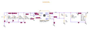
Here is the circuit I try to simulate (at first simple, without addind the extra capcitance and the ferrite):

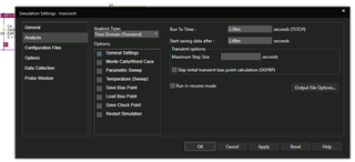
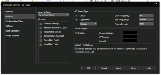
My simulation profile is the following:
And here are the curves I get:
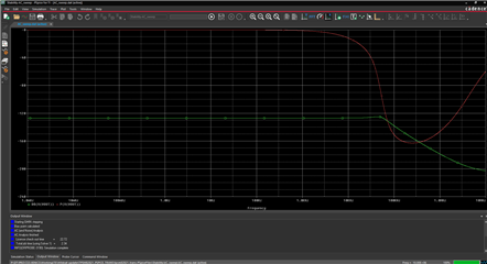
The curves seem to be completely wrong. It is not even possible to compute the phase margin (phase shift when the magnitude plot crosses 0dB). What am I doing wrong? 

Thank you in advance for your help,

  • Hi,

    Unfortunately, it won't be possible to do the AC sims with this switching transient model. An average model is required for this and we don't have one for this device.

    The best option to evaluate stability would be to run a BODE plot measurement on your board.

    The stability can also be indirectly simulated using the transient PSPICE model, by applying a fast load transient. Please check this app note to see the correlation between the output ringing cycles vs phase margin. https://www.ti.com/lit/an/slva381b/slva381b.pdf

    Best regards,

    Varun

  • Hello John,

    Thank you for the quick answer. 

    I'm not sure to understand, how can I run a BODE plot without doing a AC simulation?

    Best regards,

    Théo

  • Hi Theo,

    Sorry for the misunderstanding. I meant to run a BODE measurement on your PCB in the lab to measure loop gain.

    Best regards,

    Varun

  • I am trying to perform transient simulations but I am struggling. Are you sure this model is able to perfom transient analysis?

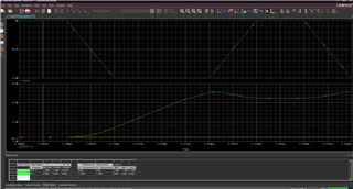
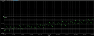
    I'm sorry maybe I miss something but I have to say that Pspice is not very intuitive, could you help me to understand what am I doing wrong? At first, why is the output voltage starting at 1.196V? With 2x 100kOhm in the voltage divider for the feedback, that leeds to 1.2V.

    Then, the output voltage seems to increase at each current step (??)

  • Hi Theo,

    For the output current source you would have to use positive values for I1 and I2. They correspond to the current flowing into the current source.

    You would have to start with some base load (~400mA) as the steady state test bench requires a few switching cycles for the internal nodes to reach the correct DC operating points. Also a higher base load is useful for the stability analysis as it's good to have the converter running in PWM mode (continuous switching) with a "closed" control loop. In PFM mode the control loop is "open" when you are in the pause (non-switching) state.

    For the load transients, it's also good to use fast slew rates so that you have a better chance to trigger and observe the ringing instabilities at the cross over frequency of the device.

    Best regards,

    Varun

  • Thank you now I can run transient simulations.

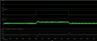
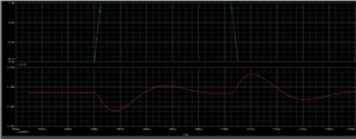
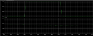
    I have a last question, as you can see in the following captures, the output voltage with the ferrite bead and the 3x 22uF capacitor seems to be very stable compared to the simulation without this extra circuit. Nonetheless, in the datasheet, it is stated that values over 47µF can degrade the stability of the converter. This is clearly not reflected in my simulations, so my question is: is it possible that your simulation model does not take into account this limitation?

  • Hi Theo,

    If you saw no ringing in the output, it should be stable. I would suggest to increase the duration of the load step to better see if there is any ringing. Also try with the load step applied before the ferrite bead at the C14 location. You need to get an undershoot in the VOUT to trigger the response of the control loop. When the load step is after the ferrite bead, you don't get a big undershoot on the rail before the bead. 

    To test the model, I ran the sims with about 110uF COUT and you can see the ringing in VOUT

    It is still recommend you double confirm stability with a BODE plot measurement on your PCB, so that all PCB parasitic are considered.

    Best regards,

    Varun

  • Hi John,

    Can I ask you what parameters/ simulation profile you use for your last simulation? I tried with only one 100uF output capacitor but the steady state is not reached even after 1ms (the simulation are so long) while in your simulation the steady state is already reached at 450us. 

    I don't see may difference compared to your circuit: (but the input/output voltage)

  • Hi Theo,

    You would need to add an initial condition (IC={VOUT}) to your cap. Double click on the cap and you will see IC as one of the parameters. The display of this is turned off by default. If needed, you can turn it on to see it in your schematic as well.

    The IC will help the output node to start at VOUT. Even with this, the model doesn't immediately settle in steady state, as I guess some internal nodes in the model don't have the right ICs. So you need a few 100us to reach steady state. 

    Best regards,

    Varun