We have used TPS61022 to boost 3.3V supply to 5V (2.5A peak, 0.6A typical) in one of our new design.
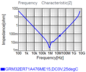
TPS61022 IC on 4 out of 10 proto boards (1st proto) failed at power on i.e., SW node short found with GND pin. Sometimes, it worked for few power cycle and suddenly found failed. 6 boards were working fine. Input source was 3.3V current limited DC supply during this testing. We are using this power supply to power up one SOM module and as per their recommended design, we have total 8 Qty 47uF (X7R 10V ceramic) in parallel (spread across board) at output (+5V rail).

We have followed proper layout recommendations as well.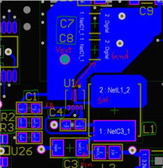
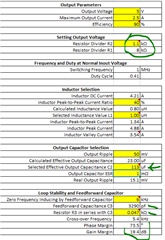
From datasheet, we found that feed forward capacitor (C1 in our design) is recommended for >40uF output capacitor design. Then we have added 1.5nF as feed forward capacitor to all our boards and no failure observed till then. 1.5nF value derived from datasheet equation. We had resistor divider value Rupper - 49.9k and Rlower - 6.8k at that time as shown in schematic snip.
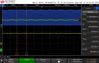
But, output voltage was dropped when we mounted SOM module (i.e., applied load). It was almost 4.65V at 400-500mA load current. Output voltage was varying based on load. Can you please explain why this phenomena happening after adding Cff? Note: We have tried different Input sources also (i.e., 6A current limit DC source and our power board 3A capable 3.3V). Also, we have tried PFM and PWM mode (mode pin low and high), seems same result. We are using PWM mode now i.e., mode pin high).
Now, we started playing with C1 (feed forward) value. We tried 1nF to 100pF and found output voltage drop reduced to 4.85V (C1 = 100pF) at same load (400-500mA). This is ok but can be issue if our load current increases based on processor application load.
Now, to reduce impact of feed forward capacitor, we reduced resistor divider value to lower side keeping ratio same. We used Rupper - 8.25k and Rlower - 1.1k with Cff = 100pf as it is. This helped and at same load current (400-500mA). Load regulation was around 2% (5V from 5.08V). Still, it is dropping while increasing load. So not sure, how to select Cff.
Need someone's help to get how to select Cff and to understand phenomena so we can get confidence to finalize design. Or do you suggest any change in design? Your early response would be appreciated.