Hello,
I've an issue with an LM5069 Load Switch on my board.
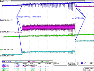
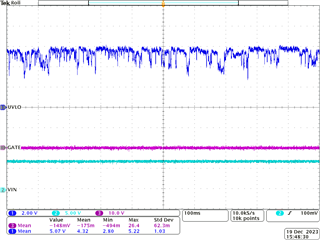
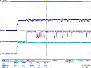
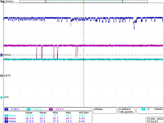
The problem is that the Load SW is supposed to enable the gate of the N-MOS at some defined point, but unfortunately, it doesn't happen. Instead, I observe a strange behavior at the N-MOS Gate. The LM5069 starts toggling the N-MOS gate at a constant frequency.
Before I continue with the issue, I'll describe my electrical system requirements:
- Input voltage range – 9V to 36V. Nominal 12V. This is also an input voltage for the LM5069
- Output current (through N-MOS) – 6.7A max
- Under Voltage – Low=11.2V, High=11.6V
- Over Voltage – Low=36V, High=40V
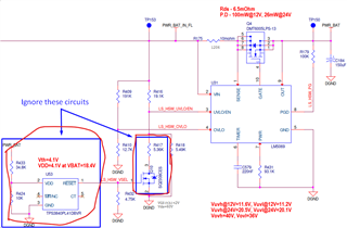
Below is the schematic of LM5069 on my board:
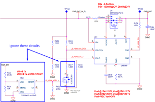
Details of the elements of the scheme (attached LM5069 design calculator with all relevant parameters):
LM5069_Design_Calculator_REV_C.xlsx
- 10mOhm for RSNS – R175
- For desired UV values as described below, I've used following resistors:
- R1=19.1Kohm – R416
- R2=5.49Kohm – R418
- Output capacitance: Cout=150uF+100uF. Total Cout≈250uF (maximum allowed output capacitance based on LM5069 DS – 350uF)
- Selected Hot Swap FET (N-MOS) - DMT6005LPS-13 (Q4). FET parameters (DS attached):
- Rds(on)≈5mOhm
- Vds=60V
- Id=125A
- Ctimer=220nF (C579), for Tfault=10.35msec
- Rpwr=93.1Kohm (R431) for a 74.5W PLIM
- System start-up condition:
- Load Turn-on threshold – 6V
- Start-up load current – 0.5A
Based on these parameters, it seems that the selected components fit my design requirements.
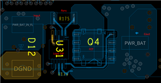
The layout was based on TI recommendations:
So, I expected to see the following graph:
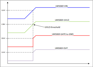
However, the actual situation is quite different. Instead of rising the Gate pin to 23.6V, the LM5069 starts toggling the Gate pin with a sawtooth signal (with a time period of 870 microseconds) at a UVLO.
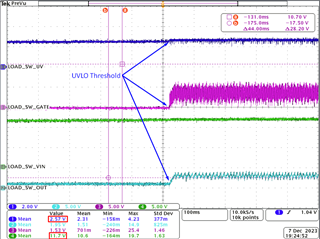
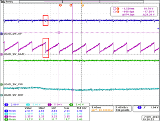
If I increase the VIN to around 13V, the LM5069 starts to act as expected.

In an attempt to stabilize the operating point, I tried to change both the Ctimer and Rpwr values to increase/decrease the Fault Time and Target PLIM, but these changes had no effect.
Please refer to the attached Design Calculator containing all design parameters (entered in green shaded cells). As mentioned below, the maximum current is around 6.7A, but during startup conditions, the current is below 0.5A at 13V.


