This thread has been locked.

If you have a related question, please click the "Ask a related question" button in the top right corner. The newly created question will be automatically linked to this question.

LM5146: SYNCIN FROM EXTERNAL SOURCE

Part Number: LM5146

What is the ideal way to drive the SYNCIN input from an external source?

Should this source be present and stable before the supply is enabled, after? Or is it inconsequential?

Should the 20K pull up to VCC be removed when using an external sync clock?

In the attached schematic, using the LTC6908IS6-1 to generate the sync input w/ the 20k pull up present, and 5V source turning on after the 3.3V supply, it causes the 3.3V supply to be unstable and not recover, until powered off and the frequency removed from SyncIN by depopulating R419.

  • Daniel,

    So the device powers up and then the SYNC clock comes in?

    Is the SYNC frequency close to the RT frequency? Have you seen the scope shot of the SYNC waveform and can you share it?

    Let me know,

    -Orlando

  • Yes, the device powers up, then the SYNC clock comes in when Vout is high enough to power the 5V boost. Sync frequency is set to the same (within 10kHz center frequency) w/ the exception that the SYNC frequency is a spread spectrum for EMC mitigation and is spread out at ±10% of the center frequency. SYNCIN is blue and 3.3V output in green. 3.3V output does not actually reach stability before SYNCIN is applied.

  • Daniel,

    Is this during the soft-start? That startup looks unstable or some variable loading.

    If the SYNCIN is removed then does it power up correctly?

    Also is the SYNC  suppose to be 5V amplitude? It looks like 4V. 

    Let me know,

    -Orlando

  • This is the waveform with the SYNCIN removed (R419 depopulated). I left the freq overlayed for timing reference only as it is not connected. SYNC should be 5V amplitude as you can see, but the 5V rail can't be boosted high enough until the 3.3V rail gets high enough.

  • Daniel,

    What is going on before the 3.3V is enabled? Before it's enabled it does not seem like the same waveform.

    Also with the SYNC signal, in one case it starts switching immediately, in the other case it does some upslope, pulls down, waits and then starts switching.

    Are you able to apply the SYNC signal after the device is powered up?

    Let me know,

    -Orlando

  • SYNC starts switching immediately in both cases as soon as the 5V rail gets over 2.7V. Then the amplitude follows its voltage input up and down while the 5V is trying to be boosted from the 3.3V.

    I ran a test where I apply SYNCIN after the 3.3V and subsequently 5V rails are up and this also caused the 3.3V rail to become unstable, as I expected, so it doesn't appear that it matters when SYNC is applied. I have also not had this issue with other TI controllers in the past with the same architecture.

     Blue is 3.3V, Red SYNCIN.

  • Daniel,

    Agreed, it appears like the sync in is actually affecting regulation. 

    If your SYNCIN frequency and the free-running frequency are the same (might be good to double-check), then the SYNC should work fine.

    There might be noise coupling from the SYNC node and interacting with the stability of the converter, does this SYNC trace route close to small-signal traces FB, COMP, SS, or RT even? 

    -Orlando

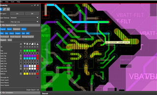
  • I highlighted SYNCIN. FB is directly beside on the right for a very short bit, but not close to any others.

    Could the spread on the syncin be an issue? It's only modulated 10% so it seems to be within the -20%/+50% nominal limits specified in the datasheet. Scope shows maybe a minimum freq of ~225kHz and max of ~275kHz.

    SyncOut looks correct, matching SyncIN, when present, and is ~260kHz when not, so Rt is set correctly.

    Any scope trace that can help? Probably won't get to it before Christmas, but can get it after the new year.

  • Hello, The responsible engineer is out of office now. TI responses may be delayed during the end year Holiday Season until Jan 2nd, 2024. Thank you for your patience.
    -EL

  • Daniel,

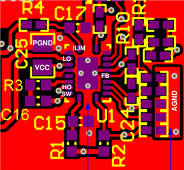
    your small-signal layout is not that great, specifically regarding FB placement and routing.

    The lower FB resistor is ideally placed close to the FB and AGND pins, to minimize noise susceptibility.

    The FB to COMP loop should also be minimized.

    Maybe you can reduce the FB impedance by lower the FB resistances 10x, this should decrease noise susceptibilty.

    However changing the FB resistors you must re-calculate the compensation values, use the quickstart calculator.

    https://www.ti.com/tool/LM5146DESIGN-CALC 

    Also see layout example and R10 lower FB resistor placement in EVM.

    -Orlando

  • I'm working on testing some new values for the compensation as you suggested. The Design Calc spreadsheet you referenced gave me different values than webench did so I will try those with the current FB values first, and if that doesn't work, then try it with the new FB values. I'll let you know how that testing goes.

  • Orlando, just changing the compensation values allows the SyncIN to be used now and the supply to be stable. Doing load testing on the supply though, the regulated voltage is being pulled down to ~3V at a 8.5A load. Do you believe changing the FB values and compensation could improve the load performance? Or is this a separate/unrelated issue?

  • Daniel,

    Is is 300mV transient drop, or 300mV steady state?

    If it is steady state, can you probe FB node voltage?

    300mV drop is expected for 35mΩ series resistance, but that is pretty high for PCB.

    Let me know,

    -Orlando

  • It was steady state. I did not probe the node voltage first, but already changed FB values and compensation. Its working great now. Thanks,