This thread has been locked.

If you have a related question, please click the "Ask a related question" button in the top right corner. The newly created question will be automatically linked to this question.

LM25066A: LM25066A - Damage to the Gate Pin

Part Number: LM25066A
Other Parts Discussed in Thread: CSD16556Q5B

Hello, 

I'm testing the following circuit. 

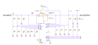
I'm having an issue similar to the one reported in this thread. I have damaged several devices during testing. The gate drive pin appears to be damaged and it is not turning on the pass FET. On the damaged devices, I measure between 1 and 200Ω on the gate pin. On a functioning device, I measure 20MΩ. 

I had some devices fail during startup and short testing. The devices worked for some time until they eventually failed. We had other devices during normal use. That is, they would have only been exposed to power cycling, no invasive short testing. 

In the related link, the suggestion is to add 10Ω in series with the gate. Can you explain why you made this suggestion? Will this prevent the damage I'm seeing to the gate pin? 

Thanks

John

  • Hi John,

    Thanks for reaching out to us.

    Could you please fill out the design calculator to review the MOSFET SOA margin? Please make sure to put the output capacitance value and the start-up load information accurately. 

    https://www.ti.com/tool/download/SNVU310

    Series gate resistance is recommended to damp the high-frequency oscillations generated by the MOSFET stray inductance and capacitance during controlled slow turn-on.

  • Hi Avishek, 

    Design calculator attached. 

    Thanks

    John

    0358.LM25066_Design_Calculator_REV_D.xlsx

  • Hi John,

    As per the operating conditions mentioned in the design spreadsheet you shared, the design looks fine to me. Please use the series gate resistance to the individual MOSFETs gate as suggested earlier. 

  • Hi Avishek, 

    Thanks for confirming. I will add the gate resistor on my next PCB revision. 

    However, I cannot make this change on my existing PCB. The gate signal is buried on an inner layer. I cannot access the trace to cut it and insert a 10 ohm resistor. Do you have any suggestions for my existing schematic? 

    In lieu of the gate resistor on my existing revision, would adding the slew rate control circuit eliminate the oscillations? I can add the circuit without cutting traces on my board. 

    I'm going to remove D35 (Vgs protection for FET) as the CSD16556Q5B is rated to +/- 20V. Is it possible that when the LM25066A switches off, the output capacitance discharge through this the gate pin and causes damage? I don't think this is likely as the resistive divider will bleed the output caps but I'm going to remove the diode regardless. 

    Thanks

    John

  • Hi John,

    Adding the slew rate control circuit may not eliminate the oscillations. 

    Output capacitor would not discharge through the gate pin. 

  • Hi Avishek,

    When the gate drives low, it has a 190mA pulldown. Won't that be the path of least resistance and discharge the caps? 

    Based on RMA with other customers, what is the source of failure when the gate pin is damaged? I have been assuming it was the zener but is it another structure? 

    Thanks

    John

  • Hi John,

    The output capacitors discharge through the short-circuit current during the output hot-short. Capacitors won't discharge through the 190-mA pull-down GATE current. 190-mA gate pull-down current activates only for a short while (~ 10 μs). 

    Mostly GATE to GND short happens.