This thread has been locked.

If you have a related question, please click the "Ask a related question" button in the top right corner. The newly created question will be automatically linked to this question.

TPS254900-Q1: Attempt to change the CDP and SDP modes of the chip in TEST_ J mode

Part Number: TPS254900-Q1

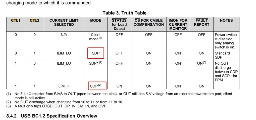
We are entrusting USB authentication, TEST_ Attempting to change the relevant configuration of the chip in J mode, the experiment found that CTL1 and 2 were set to SDP mode, and the DM voltage was measured to be 4.7mV in J mode; Set CTL1 and 2 to CDP mode, and measure the voltage in J mode as DM22.5mV;

In SDP mode, although test_ The voltage of J is low, but there are several U-disks that cannot be recognized;

Certification determination requirement TEST_ In J mode, the DM is lower than 20mV, so please help to check our schematic where there is an issue with the hardware configuration (such as current limiting resistors, etc.). Please analyze and provide support. Thank you. Attached is a schematic diagram of the design.

We tend to use SDP mode for testing_ In TEST_J mode, the voltage may be too low and pass the certification test, but we are not sure if there are any side effects, such as a decrease in USB recognition ability. We can still mount HUB outside our host, so the host does not provide fast charging to customers, and the hub provides charging function.

 ZHENKANG SCH.pdf

  • Hi Sam,

    Sorry to reply to you so late, we will have a look on this issue, and give some feedback to you, thank you.

    Best Regards,

    Kuno

  • Hi Sam,

    I don't have much experience on JK test. But here is some view.

    1. Are the eye diagram test results well?  Suggest to change C1618 and C1619 to 4.7pF.

    2. From SDP to CDP, voltage level is lifted due to bigger current which may boost ground voltage. Please check GND layout whether high voltage drop there if bad layout.

    3. Phones usually charge in CDP mode by my experience. 

    4. Check eye diagram.

  • 1. The eye diagram has been tested and has been passed. Because the eye diagram results are PASS, C1618 and C1619 do not need to be adjusted for the time being.

    2. In the mode of SDP and CDP, the current is set by us through the current limiting resistor, and the current of both settings is less than 1A output.

    3. Our products are car machine products, not mobile phone products, customers do not require direct external charging, the actual use is the car machine mounted HUB, by the HUB external charging, so it is not mandatory to use CDP mode.

    In the certification test, one of the tests TEST_J mode, the measured SDP and CDP modes of our host are lower than 20mV, (15mV in CDP mode alone, 6mV in SDP mode, and the judgment is OK), but with the partial voltage of the HUB, it will exceed 20mV in CDP mode, and it will be judged to be unqualified.

    The HUB working mode is CDP mode, it is 11mV for the test alone, and our car machine exceeds 20mV in CDP mode and it combination, so we can only choose SDP mode to work, in order to pass the test.

    Therefore, it is better to ask TI experts to explain the specific reasons, as well as the suggestions for customers in similar situations. Thank you!

  • Hi Sam,

    Do you mean after insert HUB, one partial voltage shall be introduced and leads to the failure?

  • I am confused what do you mean about these words.

  • Hi Sam,

    11mV or 20mV is so small a voltage. How to remove the effect of noise?

    I am not sure why it fails with Hub added. But from my experience, as I said before, ground shift may be one cause. Please ask Hub team for more information. They should be more professional on data transaction.

  • we focus on Test_J mode voltage,but not noise

  • Hi Sam,

    Got it. Have never received test_J cert from customer before. Shall learn more about it and discuss with you.