A related question is a question created from another question. When the related question is created, it will be automatically linked to the original question.
If you have a related question, please click the "Ask a related question" button in the top right corner. The newly created question will be automatically linked to this question.
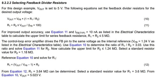
It would be good to reduce the feedback divider values to avoid the inaccuracy in LDO output when the divider current becomes comparable to the FB pin leakage.
It is expected to R1 + R2 < 5 Mohm
This is discussed in details in section 9.2.2.2 Selecting Feedback Divider Resistors of the datasheet.
As mentioned for 5V output, R1 can be 3.64Mohm and R2 can be 1.18Mohm.