This thread has been locked.

If you have a related question, please click the "Ask a related question" button in the top right corner. The newly created question will be automatically linked to this question.

TPS63710: Unstable Operation of TPS63710

Part Number: TPS63710

Hi,

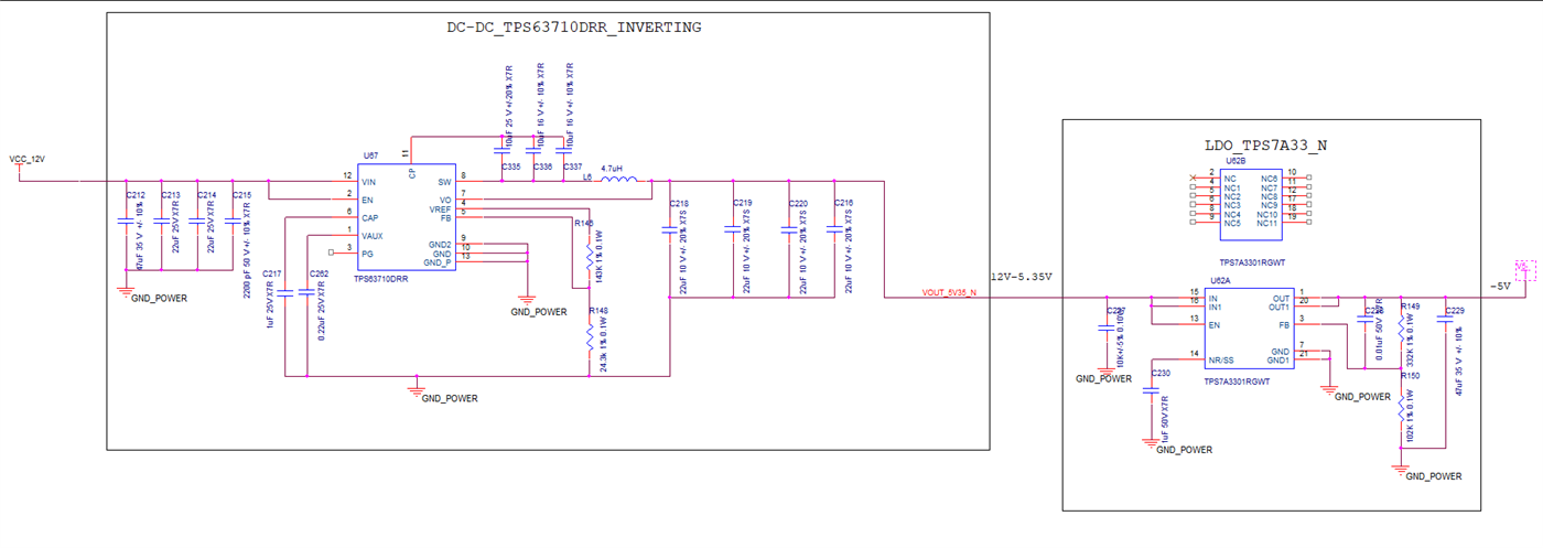
I have got reviewed the schematic and layout here

TPS63710: TPS63710 Layout Review - Power management forum - Power management - TI E2E support forums

TPS7A33: TPS7A3301RGWT Layout Review - Power management forum - Power management - TI E2E support forums

Now i have got the realised board in my hand 

What i am observing is quite strange after a minute of time the power ic keeps on restarting and the output voltage is not stable as the output is off for a while, kindly let me know where exactly the problem might be wrong with my schematic ?

i am reposting the schemati again below

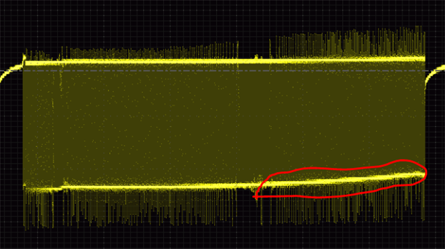
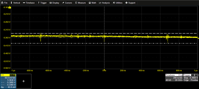
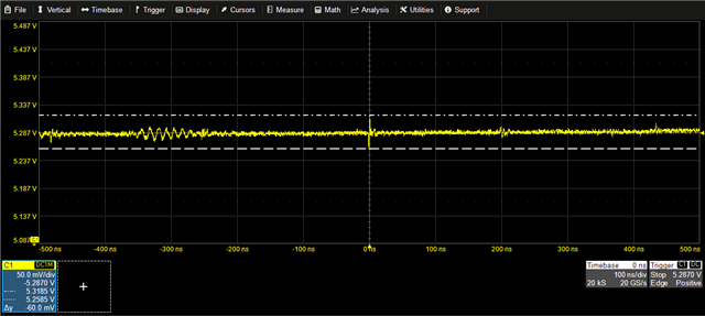
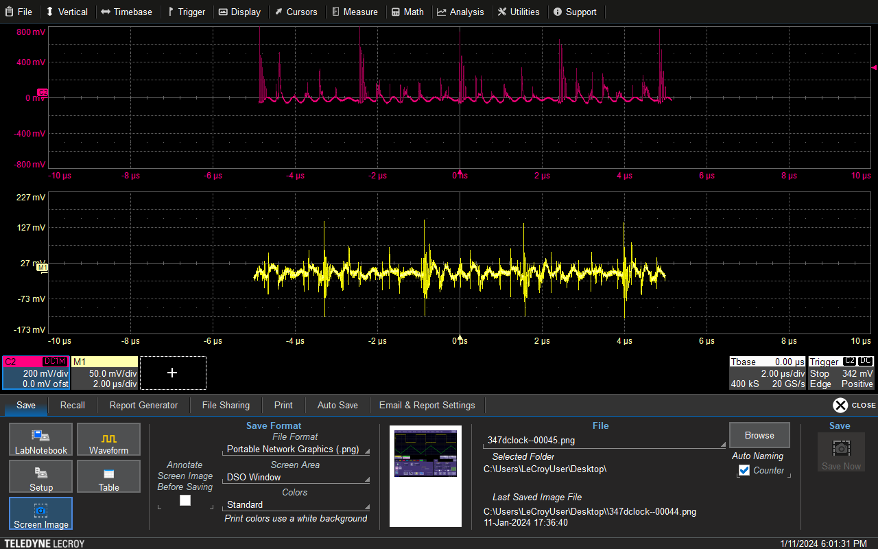
The wavefrom of SW is as below

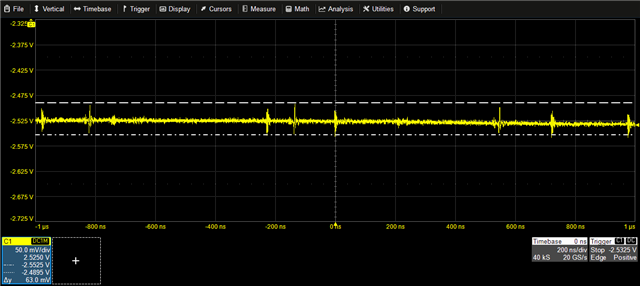
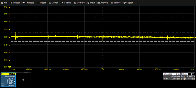
Waveform of CP is as below

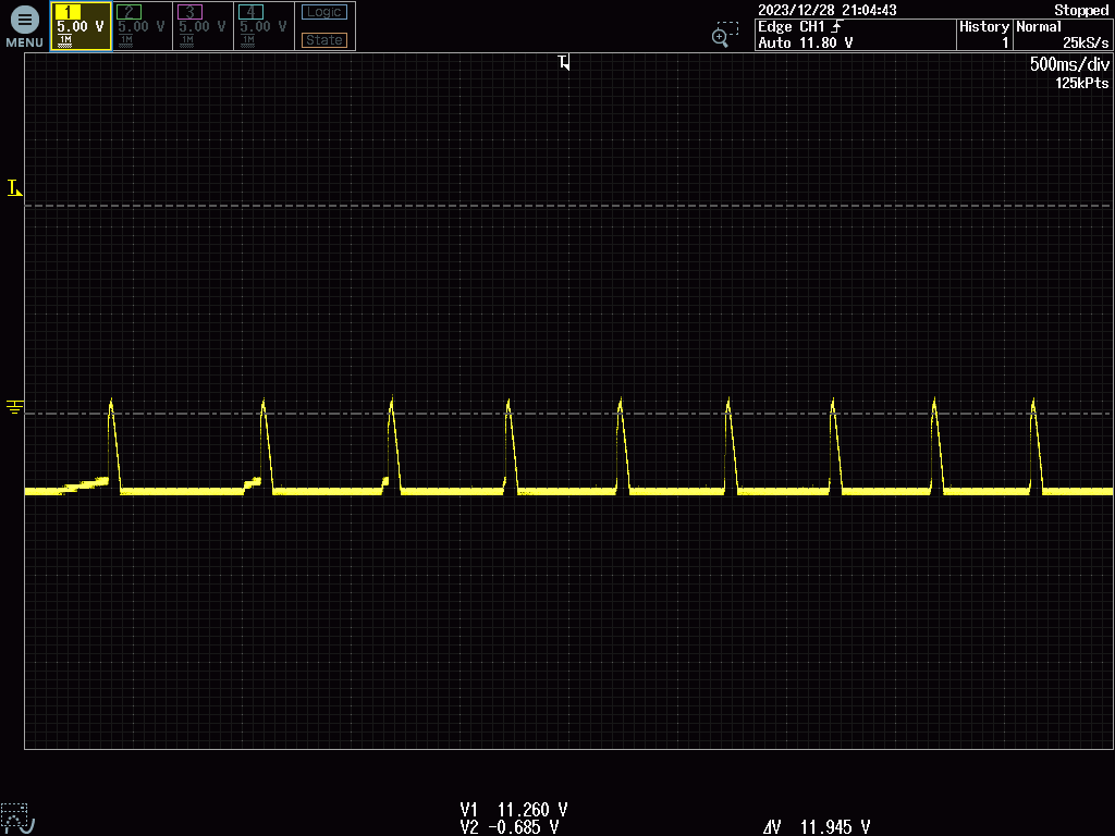
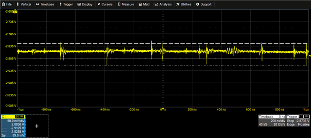
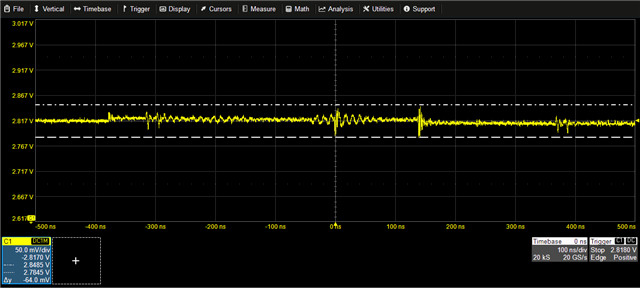
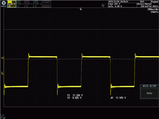
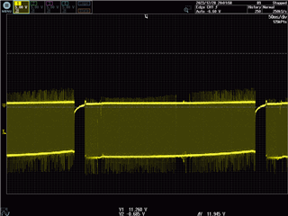
After a minute of time i observe the waveform like below in long time-scale which is a clear indication of restart of regualtor and there by heating the board so much

1. Suspecting C219 and C220, i have removed the extra 22uF Capacitance

2. C215 is also removed as its wrongly put with small value

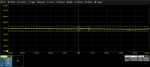
Still the output remains the same at SW

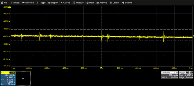
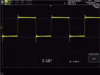
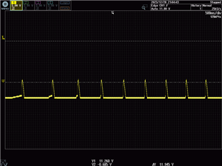
eventually the output at DCDC is as below

Is there anything wrong in the schematic which is creating this issue, kindly help

NOTE : a similar approach i have used for creating -2.85 followed by LDO to create -2.5V in which there is no issue, but this higher negative voltage is creating the issue.

  • Hi Shyam,

    Thanks for your enough waveforms. It looks the device restarts.

    There're three possible reason causing restart. Input voltage UVLO, output current limit and over temperature.

    1. Input voltage UVLO is not possible since the SW voltage is ~12V during on-time.

    2. Output current limit is possible since we can see the input voltage is decreasing before restart.

    To confirm whether it's due to output current limit, you can try to probe the inductor current.

    You can catch it by disconnect one side of the inductor and use a wire in series to catch the current using a current probe.

    3. Over temperature(OT) is possible since we can see the keeping time is shorter and shorter and that's may be related to the temperature.

    If you can see the keeping -5V time is long just after first powering up and becomes shorter and shorter then, the OT is a possible reason.

    It would be better if you have a camera to catch the case temperature.

    Waiting for your response.

    Athos

  • I have seen a blunder happened in my assembly, i have the output 47uF cap changed to tantalum at last minute due to unavailablity of ceramic

    the tantulum cap is mounted reverse, postive terminal of tantalum is connected to negative ouput of LDO,due to this it heated so much and spread the heat all over board, i observed this quickly with a thermal camera and reversed it, with which the issue resolved

    below are the waveform of output

    -5V LDO output :

    -5.35V DCDC Output

    -2.5V LDO Ouput

    -2.85V DCDC Output

    5V LDO Output

    5.35 DCDC Output

    +2.5V LDO ouput

    +2.85 DCDC outuput

    1. I see the DCDC which is generating +2.85V is being excessively getting heated up, is there a way to reduce this heating ?

    2. Also can you see the output switching noise levels if are they as per expectations in datasheets ? i feel i can come down much less of switching noise, placing few extra caps at dcdc output will it reduce the noise ? suggest few methods.

  • Hi Shyam,

    Good to know the issue is solved.

    Regarding you questions:

    1. To reduce the heating, you can optimize the layout by expanding the GND area and adding some more GND vias. However, I see you've already placed some vias on GND plane. What temperature do you see on the IC top case? Is it out of spec or without enough margin?

    2. The switching level is good as long as the voltage of VIN, CP and SW is within below spec.

    If you still want to reduce the switching noise, there are several methods as below.

        a. Add a 100nF input capacitor near the VIN pin and GND pin.

        b. Add a RC snubber between CP and GND.

  • Unfortunately this noise is appearing in my opamp circuits as i am operating at very low noise levels

    can you explain or throw some literature about adding snubber and 100nF caps at inputs ?

    This would help me to tackle the noise better

    For example the yellow one is the first TIA  of gain 10K and pink is Inverting amplifier of gain 10, which has this spurious pulses, i am pretty sure the noises are from power supply and no photo diode is connected, i wish to bring down these noises at opamp to much low.

  • Hi Shyam,

    The two ways I shew you are to reduce the switching noise but here you mentioned is the noise of output voltage. I'm not sure if they are related. Sometimes yes, but I want to first confirm that.

    Usually output noise our customer tested is from the probe but not actual noise. You can try to measure the ripple using a pig tail to reduce the space injection. Also you can follow this AN. https://www.ti.com/lit/ta/ssztb25/ssztb25.pdf 

    The switching noise means the ringing during FET on/off. You can refer to below AN about RC snubber.

    https://www.ti.com/lit/an/slyt465/slyt465.pdf 

    Also the noise is highly related to the layout, you can send me the layout for review, too.

    https://www.ti.com/lit/ab/snva803/snva803.pdf 

    Regarding the noise issue, you can firstly use a pig tail to measure the OPA voltage. If the noise still exists, you can disable our DC/DC and change it  to a DC source to see if the noise is gone.

  • please can you drop a personal msg with mail id, i shall mail  you the layout file to your mail.

    Infact i was measuring noise at output of dcdc and opamp with nearest ground using a pigtail probe only.

  • athos-zhao@ti.com