


Hello there,
This is Prit, I am trying to design an DC-DC converter using LM51551 IC, I am attaching Schematic of my design.
Design parameters are as below:
Input voltage : 8V to 36V
Output Voltage : 12V Fix
Max Output Current: 5A
Topology used : SEPIC
When i am drawing not current from this designed supply its working fine, 11.89 V output I am observing, and its quite acceptable ripple with whole range of input voltage (8V - 12V).
But when i am drawing current of 1 Amp from it its getting tripped by Hiccup mode at input voltage of 17 V When i am using Mosfet IRFB3077, and i am being able to draw 3A at 17V input with MosFET IRFB3205
At this mentioned current of load i am not being able to go below 17V in input
Calculator and references used for this designing :
Reference calculator excel sheet
Datasheet & AN-1484 Designing A SEPIC Converter
What are my questions ?
1. Even if IRFB3077 is having low Rds_on, Why its performance in circuit is lower then IRFB3205?
2. Even if all calculations seems to be right and done using Excel sheet provided by TI, I am not being able to get 12V @ 5A with 8.5 V of input supply ?
3. Why mosfets are heating up too much?
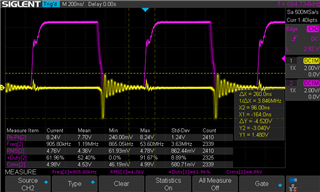
4. When i am observing waveform of voltage across sense resistor 0.005 Ohm (3W, also checked), i am getting Spike of 0.8V to 3 V which is equivalent to 100s of A running through it, And my supply is just capable of providing 10A max
(I didn't observed supply getting tripped or CC mode because of these spikes)
5. Any other Circuit topology or Better IC to fulfil this requirements?
What I have tried ?
1. I have tried different Mosfets and replacing inductors with same kind of new one
2. Checked and verified calculations again and again
3. attaching screenshots of DSO here (yellow : voltage across sense resistor, Pink : gate voltage)
(Note: This DSO measurement has been taken using ground spring probe)
It would be very helpful for us if anybody can suggest some improvement or guidance
Thanks and Regards
Prit Varmora

