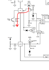
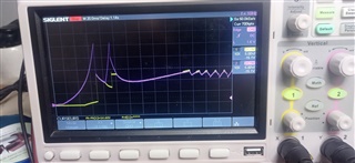
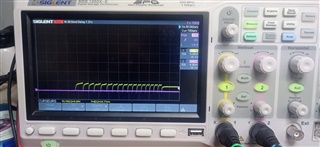
Why i obtiend 0V on FB given that LL/SS pin gives me 5V
This thread has been locked.
If you have a related question, please click the "Ask a related question" button in the top right corner. The newly created question will be automatically linked to this question.
Hello Abdellah,
Can you please elaborate on your problem and give a schematic, waveform, etc.? As you can see by the internal block diagram, the voltage of FB will depend on how much current the FB pin can source and should not depend on the LL/SS pin voltage.

If you are seeing no voltage on the FB pin, it is likely because the optocoupler is open, which means your feedback loop is designed incorrectly.
Regards,
Jonathan Wong
Bonjour Jonathan,
je vous remercie pour votre réponse, vous trouverez ci dessus un tableau qui résume tous les composant utilisé dans le circuit.UCC25640x Design Calculator Rev5 (version 1).xlsx
Voici aussi les résultats obtenus sur l'oscilloscope pour VCC, RVCC dans IMG1 , et FB , LL/SS dans l'image 2


Hello Abdellah,
Placing English translation below for future reference and searchability:
"Thank you for your answer, you will find above a table that summarizes all the components used in the circuit. Here are also the results obtained on the oscilloscope for VCC, RVCC in IMG1, and FB, LL/SS in image 2"
To clarify the oscilloscope captures, is the following correct?
Image 1
Image 2
Please keep all E2E posts in English and not French. TI only offers E2E support in English and Chinese. We will provide an answer shortly.
Regards,
Jonathan Wong
Hi Abdellah,
Please ensure that the resonant tank meets the maximum gain requirement. The maximum gain obtained in your design does not meet the maximum gain criteria.

After you fix the tank parameters, please use the debugging guidelines given in the following app note for tuning components around the controller.
https://www.ti.com/lit/pdf/sluaaj7
Regards
Manikanta P
Hi Abdellah,
What do you mean by this?
yes, it was like you mentioned
Regards
Manikanta P