This thread has been locked.

If you have a related question, please click the "Ask a related question" button in the top right corner. The newly created question will be automatically linked to this question.

LM5156H: Boost circuit Issues

Part Number: LM5156H
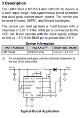
Other Parts Discussed in Thread: LM5156

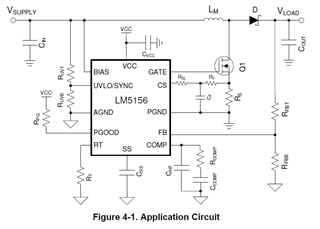
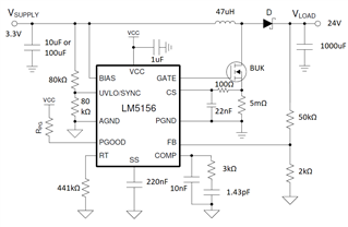
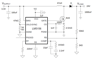
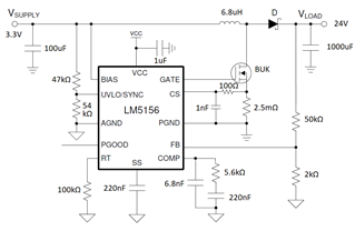
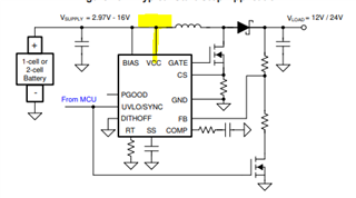
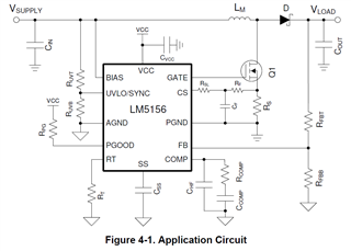
We have been designing a boost circuit to take a 3.3V @30A source up to 24V @ 2A. I went through the calculations within the "How to Design a Boost Converter Using the LM5156" instructions, but ran into a couple hiccups throughout the actual implementation. The design is shown below:

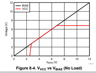
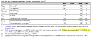
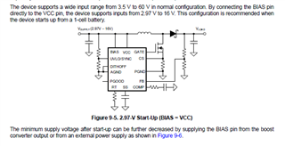
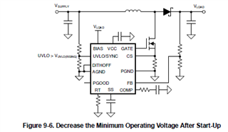
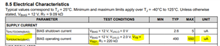
The design has Vcc decoupled from the Bias pin, but in the datasheet there is a configuration where they are connected. There is also these notes about Vcc and the Bias pin:

Since our input is 3.3V, The notes show I should connect the two, but this isn't shown on the boost calculation guide. Below is our calculated values for our design. Please let me know if something doesn't look correct, I am struggling to find where this is going wrong.

  • Hello,

    Thanks for using the e2e forum.
    The datasheet lists a restriction that VCC should never higher than VBIAS.
    This is due to an internal ESD protection diode that goes from VCC to BIAS. If VCC > BIAS (+0.3V), the ESD diode would be conducting current from VCC to BIAS and will take damage, as it is not meant to support larger current flows.

    If VCC is just connected via a cap to GND, there is never any risk of higher VCC voltages.
    When operating with Vin of 3.3V, please note that the gate driver voltage will also be 3.3V, which has to be enough to fully turn on the switching FET.
    If the voltage is to low to support the FETs, you can consider an external supply at BIAS or a flyback implementation, where VCC is boosted to a higher voltage as well.

    These implementation are described in the chapter 9.3.2 of the datasheet:

    There is also a workaround solutions for VCC > BIAS.
    Please implement a forwarding diode at the input of the BIAS pin. This diode will block any reverse currents from VCC to BIAS and will allow a higher VCC voltage.

    Best regards,
    Niklas

  • Niklas,

    Thank you for the response! We aren't having any issues with the Vcc pin being higher than the BIAS pin. When we run the circuit with the battery connected to BIAS and a capacitor from Vcc to ground, the gate pin does not seem to be activating at all, and measuring at the Vcc pin gives almost no voltage. When we connect the two pins together as shown in the diagram below, we see a voltage on BIAS/Vcc, but the gate output is not present on our scope.

    Let me know if you have any experience of using this with a lithium battery. We are struggling to find a boost controller to fit our application and I am more worried that either we don't have enough voltage on the chip or some of the values I calculated are incorrect and the chip is in some sort of shutdown mode I can't seem to fix.

    Brian

  • Hi Brian,

    Thanks for the update and clarification.
    So there is no gate signal after startup and the VCC is close to 0V.
    In theory, the VCC voltage should follow the BIAS voltage in the range from 3.5V to 7V.

    As you already pointed out in the initial post, the electrical specs mention a minimum BIAS supply of 3.5V for proper operation.

    When supplying with a 3.3V battery, I am afraid the voltage might be too low to turn on the device.

    Do you have the schematics of their application?
    We might find some other errors when reviewing their design.
    Otherwise I would ask for waveforms of their BIAS, VCC and gate voltage, so we can check if the device is active or still in shutdown.

    Thanks and best regards,
    Niklas

  • Niklas,

    We are using the schematic from the "How to Design a Boost Converter Using the LM5156" shown below. I have also attached our values we are using for the circuit:

    We have yet to get any real output on the gate pin, all we see is some fluctuations around 100 mV. The description on the first page of the datasheet states we can use a one cell lithium battery to operate the device as long as it is above 2.97V as well as connecting the BIAS and VCC pins:

    The below schematic shows the recommended use with a single cell battery:

    Our goal with this is to make a 3.3V battery at 30A power a 24V load at 2A for at least a minute. The battery can support 30A for about 1 minute before being depleted. since we will be nearing the 2.97V threshold toward the end of the battery life, we can try to design our circuit to match figure 9-6 and allow it to boost to the battery's minimum voltage (2.5V) where it should shut off. Figure 9-6:

    Please review my values I attached earlier and let me know if anything could be causing an issue with the shutdown modes of the device, or if anything affects how the device should run. 

    Thanks,

    Brian

  • Hello Niklas..... Bryan (Tracy) has left for the day and I advised I would follow up on this. I believe we have two issues we'd like to get some guidance on:

    1) All through the documentation there are references to analog ground and power ground. The way the symbols are utilized is not very consistent throughout the multi-page product guide. There are even references to power ground INSIDE the chip, but no definitive connection to the outside. So, should we consider that all ground connections, regardless of power or signal, can be connected together (basically connecting the wider, shorter power ground traces to the signal grounds)?

    2) We had calculated the necessary components to utilize a 47uH inductor with a 52kHz gate frequency. We're moving to a smaller inductor operating in excess of 100kHz per the 5156H specifications. We're also re-running the support component calculations to correct for the higher frequency.   

  • Hello,

    Thanks for the update and the schematic values.
    I put the values into our quickstart calculator and found some points to optimize:

    - the switching frequency is set via the RT resistor to 50kHz. The minimum fsw per datasheet is 100kHz. Please increase the fsw to the datasheet range, as operation out of spec can lead to unexpected behavior
    - The compensation network might be unstable. Please adjust the values for Rcomp, Ccomp and Chf to create a stable loop compensation. (Also make sure that Ccomp and Chf are not mixed up)
    - The time constant of the RC filter at the CS pin is rather high (22nF, 100Ohm). I would recommend to reduce the capacitance so the current sense signal is no over-filtered. E.g. 100pF cap should be a better starting value.

    The calculator can be downloaded here:
    https://www.ti.com/tool/download/SNVC224

    I recommend optimizing the schematic and check if the device can start up.
    Please also make sure that the FET can work with a gate voltage of 3V - 3.3V and will fully turn on every switching cycle.

    Best regards,
    Niklas

  • Niklas,

    I changed a large portion of the values to be more near the 200 kHz frequency the device is capable of operating at. I changed the inductor out for a 6.8 uH 30A inductor. Below is a wave we are getting on the GATE pin:

    The frequency is bouncing around 200k, however the waveform itself is clearly having an issue outputting a square wave. 

    With the calculation adjustment to 200 kHz, I altered the values for the COMP circuit, Rt, and the CS circuits. I also altered UVLO to be better aligned with the battery voltage. The new values are shown below:

    Let me know if this is similar to anything you have seen and any ways to approach this.

    Brian

  • Sorry I forgot to adjust a few values, corrected below:

  • Hi Brian,

    Thanks for the update and modifying the circuit.
    The frequency bouncing you see on the gate signal should come from the frequency dithering function of the device. This feature can be disabled and enabled via the DITHOFF pin.

    As you mentioned, the gate signal should have a square wave instead of the spikes you are seeing.
    Just for clarification, is the current design connecting VCC to a cap, or the VIN as in a previous image you sent?

    Could you also send waveform measurements of VCC, SS and CS, so we can further look into what keeps the device from operation as intended?

    Thanks and best regards,
    Niklas

  • Below are the requested waveforms.

    Vcc

    CS

    SS

    The Vcc pin looks steady except for the slight 200 kHz fluctuations when the chip seemingly tries to operate. SS is very steady with minor changes in the signal, and CS looks similar to the GATE pin. 

    We are using the diagram you have shown with the VCC pin connected to the BIAS Pin. I currently have DITHOFF connected to ground. We are getting in some SOIC to DIP boards today to try out in case there are any issues with our connections currently. I will send an update later this afternoon.

    Brian

  • Hi Brian,

    Thanks for the update and the waveforms.
    The CS pin voltage does not look like it is supposed to be.
    The LM5156 device has a overcurrent threshold set to 100mV.


    It looks like this limit is exceeded every switching cycle.
    There is an initial blanking time to avoid false triggered due to noise, but even the oscillation after the initial peak goes above the OCP threshold.

    As you already mentioned, the VCC voltage dips slightly whenever the device tries to operate. If these dips go below the 2.97V enable threshold, the device is at risk of shutting down.

    Can you make a measurement without load connected and check if the device is able to boost?
    This would show us if the device cannot handle the load conditions, or if this is a general problem of the application.

    Thanks and best regards,
    Niklas

  • Niklas,

    We made a couple variations just to get the device to work and have still had no luck. See below:

    1. We added a second battery cell, this isn't intended to be designed this way, we just want to make the device function how we expect. Adding the second cell brought BIAS and Vcc up to 6.6V, but we were still getting the same signals as before.

    2. We removed the load and left the output open. The voltage slowly climbed and we saw the same waveforms again.

    3. We added a 1k slope resistor for the CS pin to reduce the spike, this has also done little to negate the CS pin from going above 100mV.

    4. We removed the filter at the CS pin altogether and had no change.

    The high voltage we are getting at the CS pin is strange since our shunt resistor is .0025Ω, and we are getting 400mV which would mean a very large current, but that isn't apparent. Is there a way I can contact you directly or set up a call with you to discuss this in more detail? Going through our findings and waiting an entire day is taking its toll on our schedule.

    Thanks,

    Brian

  • Hi Brian,

    I am really sorry the debugging drag on over a long timespan.
    To speed up the support, we can set up a call as well. I got already contacted internally on this, so further communication will be over mail.

    In the meantime, I made some additional comment on your newest test, that will be shared to you over mail, too.
    I put them here as well so it reaches you faster:

    - The actual schematic of your design never have been share and only values for the reference example are given.
    If you could share the real schematic design, I can check if there are any additional connections that are wrong, and also check if the inductor, FET and diode are suitable parts.
    It is also possible to share the part numbers of these three components, which would already be helpful.

    -The current sense pin is essential for the current regulation, so it cannot be removed. If there are large overshoots on this pin, they would either come from noise or from actual high current spikes.
    As you already tried several filter changes without any change in results, the peaks might actually come from high currents of the battery cells.
    Do you have an electronic power supply you can connect to board instead of the battery cells? A test with a stable supply would show if the FET can generally work with a 3V gate driver and also if the current spikes measured on the CS pin are coming from the design or the battery supply.

    Best regards,
    Niklas

  • Niklas,

    We have been testing more with the LM5156 running at our expected load current of 2A, and we have hit another roadblock. Originally when powering the device with a single lithium cell, we were struggling to turn the FET on and off completely. We switched to two cells to see if the voltage was the issue and the device ran perfectly. For our application we are making a battery back-up that is supposed to trigger on power loss. We only really have space for 1 cell, since adding another increases the circuitry for charging. 

    We wanted to try an RC circuit to supply the device since the BIAS current is only 580 uA max, but when we tested it the device is taking around 30 mA. Can you give more information on this or are the two chips we are using possibly damaged? Looking forward to your response.

    Thanks,

    Brian

  • Hi Brian,

    Thanks for the update.
    You are correct that the datasheet lists a BIAS operating current of 550uA max.

    However, this is only the current consumption when the device is enabled, but not switching.
    The test conditions lists that Vfb is pulled up to the Vref voltage, meaning the device is active but no switching is happening.
    If the device is actually boosting, this current consumption will increase.

    Best regards,
    Niklas