This thread has been locked.

If you have a related question, please click the "Ask a related question" button in the top right corner. The newly created question will be automatically linked to this question.

UCC5350: UCC5350 SCH&PCB Layout Check

Part Number: UCC5350

Hi Tier,

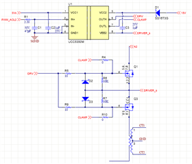
I would like to discuss the SCH&PCB layout for UCC5350M.
Could you help recommended the SCH&PCB Layout when MOSFET placed by back to back.
1. the CLAMP of UCC5350M connected after Rg.ext, right?
2. there is need the individual resistor to separate trace? Because I realize the if no CLAMP resistor cause trace and net name are same, right?

  • 1. Yes, the clamp pin should have 0 ohms to the gate capacitor.

    2. When you drive two switches in parallel, usually people prefer not to short all of the gates together. It might lead to less even current sharing. 

    However, in this case the two switches are in series so it should not be a problem. It is not clear to me how a bootstrap circuit will work for negative bus voltages; you might need to use an isolated bias supply for this gate driver.

    Best regards,

    Sean