This thread has been locked.

If you have a related question, please click the "Ask a related question" button in the top right corner. The newly created question will be automatically linked to this question.

UCC28950: Operation at light load

Part Number: UCC28950
Other Parts Discussed in Thread: , UCC2895

Hello,

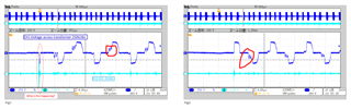
The waveform in Fig1 can be seen every few times during burst mode under light load.
What is this happening?
I usually use Fig2 most of the time.
Is this normal? Are there any countermeasures?
I'm working on increasing the efficiency of light loads.
I think it would be even better if this was removed.

regards

 Wave form_Light Load.pdf

  • Hello,

    I am reviewing your inquiry and will get back to you shortly.

    Regards,

  • Hello,

    Please note both of your waveforms have excessive ringing on the transformer that should not be present.  You may want to figure out what is causing this ringing and remove from your design.  This could be caused by layout/schematic errors.

    In Figure 1 you are correct that the polarity across the transformer should change every other cycle including burst mode.  So you should not see that behavior. 

    There is a 600 W reference design using the UCC28950, UCC28950EVM-442 that you may want to order and evaluate. The following link will bring you to the user's guide for this evaluation module.  There is a schematic, layout and test data in this User's Guide that you may want to evaluate.  https://www.ti.com/lit/ug/sluu421a/sluu421a.pdf

    The waveform below was taken from the 600 W UCC28950 evaluation module. CH1 is the voltage across the transformer and shim inductor.  CH4 is the CS signal and CH2 and CH3 are the low side FET gates.  From these waveforms you can see there is not excessive ringing that is present in your waveforms.

    The User's guide has what the behavior should look like in burst mode.  Below in figure 23 is the behavior that you should observe in burst mode.  The voltage across the transformer should change polarities every other cycle.

    When looking at your waveforms in light load burst it looks like you minimum duty cycle is set for 40%.  This is kind of high and may be causing some of your issues.  Pin Tmin of the UCC28950 sets the minimum duty cycle before bursting.   You might want to set RTmin to 10 k ohm to see if the issue goes away.  This will give a minimum duty cycle of 50ns*(switching frequency) before bursting.

    The following link will bring you to an application note that goes through the step by step design process of phase shifted full bridge using the UCC28950 PSFB controller.   There is even a link inside the application note to an excel design tool that uses the same equations as what is presented in the application note.  You can use both the application note and excel design tool to design to check your design. 

    https://www.ti.com/lit/pdf/slua560

    Regards,

  • Hello

    There was a lack of explanation.
    This power supply is a variable power supply.
    The maximum is 120V.
    The waveform this time is the waveform when the output is 50V/0.1A.
    I thought that because the OFF period was long, the energy of L on the secondary side was gone and it was resonating.
    Is it abnormal even considering the above?
    I'm starting to feel anxious.

    Also, the shim inductor is set to 10uH.
    Will ringing like this occur if the shim inductor is too large?
    In the Excel design tool, it is 1 to 4 μH.
    Excel design tool is used.
    However, because the output range is wide, it is difficult to judge whether it is correct or not.

    RTmin value is 15kΩ.
    However, the ON width is approximately 1.44usec.
    Even if you lower the resistance value, it will not become any shorter.
    What is it attributed to?

    I checked the gate signal of UCC28950.
    In the waveform discussed earlier, it seems that the delayed MOSFET (OUTD) turns OFF first.
    There is a delay in the attached gate signal because there is a driver IC and drive transformer ahead of it. We will send you the circuit diagram.

    Please let me know if you find out the cause.

    Wave form_drive signal.pdf

    1881.Circuit.pdf
       

  • Hello,

    Your inquiry is under review and I will get back to you shortly.

    Regards,

  • Hello,

    You could be right about the inductor resonating because the inductor is gong DCM.   You can verify this by studying the inductor current versus the waveform that you have taken to verify this.

    The shim inductor will form a voltage divider with transformer primary magnetizing inductor.  As long as the value is not too large it should not cause an issue.  I would think if it was 10% or less compared to Lm it would not cause an issue.

    If your RTmin is set for 15 k ohms your minimum voltage applied the transformer should be 75 ns.  Even though the controller is bursting it may not be due to light load bursts controlled by tmin pin .

    You might want to study COMP, CS, SS and the voltage across the Transformer and Shim inductor.   This may give you a clue to why the design is bursting.  

    I reviewed the schematic that you had attached and see that is of the power stage, H Bridge Driver and the current sense transformer; as well as, the output rectifiers.  The controller section and output filter was not present.  I see that you have snubbers across the output rectifiers that could be used to dampen the DC ringing that you observe across the primary of the transformer.  This may help with EMI as well.

    I also noticed that you used clamp diodes between the shim inductor and the primary of the transformer.  A log of engineers miss this and they are required to protect the secondary rectifiers from over voltage.

    Regards,

  • Hello

    There was an error in the waveform sent yesterday.
    OUTD turned on first, then OUTA.
    It seems that there is no difference in operation as long as OUTC and OUTD are advanced.
    In the catalog, OUTA and B are progressing.
    Is this behavior normal?
    If it is abnormal, what is the cause?

    Also, when I took the waveform again, Duty control was possible.
    I'm worried because I haven't changed anything.
    Which constant is effective for reviewing the drive?

    However, I feel that if the Duty is lowered any further, the loss during light loads will increase.
    If so, is there a problem if I set TMIN to 1usec? (RTMIN: 100k~200kΩ)

    Also, the ringing was due to L on the secondary side.

    We will also send you the circuit for the control section.


     regards

    Wave form_drive signal_Retake.pdf

    Circuit_control.pdf

  • Hello,

    Your inquiry is under review and I will get back to shortly.

    Regards,

  • Hello,

    In your first waveform you have OUT B, Out C and the transformer input voltage.  This waveform does not show B and C on at the same time that corresponds to voltage across the transformer.  Are you sure this is Out B and Out C in this waveform?  If it is you have something connected wrong in your H Bridge.

    The second waveform has OUT A, OUT C and the transformer voltage.  This will not show when voltage is being applied across the transformer.  You would have to look at OUT A, OUT D and the transformer input voltage.

    The voltage across the transformer should align with the A and D outputs and the B and D outputs.  When A and D are on at the same time there will be voltage applied across the transformer.  When B and C are on at the same time there will be voltage applied across the transformer in the reverse direction.

    In regards to the behavior typically voltage across the transformer will alternate.  In the waveform you are showing there appears to be a small duty cycle in the negative direction.  Shortly after it is negative again for the normal duty cycle.  Having voltage applied  transformer applied in the same direction  for two consecutive cycles is not normal. 

    What I recommend for you is the following.

    1.  Double check the waveforms you took to make sure the duty cycles are correct and line up with the corresponding outputs.

    2.  Double check your schematic to make sure the H Bridge is connected correctly.

    Regards,

  • Hello

    sorry
    The second waveform is the A and D OUT signals.
    Since both are outputs from the IC, they are not synchronized with the voltage across the transformer due to the influence of the subsequent drive IC and drive transformer.
    Also, you say that you cannot see ON at the same time, but the sections indicated by the arrows are ON at the same time.

    As the first person pointed out, I heard that it is not normal for the voltage to be applied to the transformer in the same direction for two consecutive cycles.
    At that time, I received advice that the cause might be that the TMIN was not narrowed down.
    The previous report stated that it was found that the duty of IC output was reduced.
    Therefore, I wanted to ask a question about which constants should be reviewed among the peripheral constants of drive transformers and drive ICs.

    I checked the circuit and pattern and found no problems.
    Did you have any problems with the circuit you sent?

    Also, please answer the question I asked the other day.

    ① Am I correct in understanding that it doesn't matter whether OUT_A, B or OUT_C, D are turned on first?
    (Does A turn on more than D in terms of IC operation?)

    ② Is there any problem if I set TMIN to 1usec? (RTMIN:100k to 200kΩ)

    regards

    Wave form_drive signal_Retake2.pdf

  • Hello

    I understand why the ON timing is strange.
    I think the cause is probably the back electromotive voltage of the drive transformer.
    This power supply is required to have pollution level 3, so the coupling of the transformer is poor. Even if you fix the transformer, it won't change much.
    I would like to suppress this back-induced component, but is it okay to put an SBD between the gate and source?
    If you have any other measures, please let me know.

    regards
       

  • Hello

    You looked at the voltage across the transformer and said that the ON width was not narrowed.
    However, if the load is light, energy remains on the secondary side of the transformer, so it may not be possible to determine the actual ON width based on the voltage across the transformer.

    The load factor is about 1%.


    Also, please answer the question I asked the other day.

    ① Is there any problem if I set TMIN to 1usec? (RTMIN:100k to 200kΩ)
    ②I would like to suppress this back-induced component, but is it okay to put an SBD between the gate and source?
    If you have any other measures, please let me know.

    regards

  • Hello,

    Your inquiry is under review and I will get back to you shortly.

    Regards,

  • Hello,

    If both phases are not free wheeling the voltage across the transformer will be the on time.  If you wanted to determine the exact on time based on the UCC28950 controllers, you would have to look at Out A .. Out D.  When Out A and Out D on at the same time this will be the on time from the UCC28950.  When Out B and Out C on at the same time this will be the on time from the UCC28950.

    1. In regards to setting the minimum TMIN I would recommend only using resistors between 10k and 135k ohm.  This is where TMIN was characterized.

    2. There is a DCM pin that can be used to turn off the FETs before the current goes discontinues.  This is set with a resistor divider from Vref to the DCM pin.  If the peak current on the CS pin does not go above the DCM threshold the SR FETs will be disabled.  Setting up this DCM comparator is covered in section 7.3.12 in the data sheet.

    Regards,

  • Hello

    Thank you for answering.
    My power supply is diode rectified on the secondary side.
    Am I correct in understanding that lowering the DCM value changes the load to CCM mode from light load?
    I'm currently having trouble with the heat generation of the MOSFET in the load region that switches from DCM mode to CCM mode.
    Regarding wide output voltage range
    Should the DCM settings be made at the lowest voltage in the following cases?
    Minimum voltage (minimum power) 30V/10A
    Maximum voltage (maximum power) 100V/12A

    I have another question.
    This is about when it is driven by a drive transformer.
    Is there a problem if I add a Schottky barrier diode between the gate and source of the MOSFET?
    (Direction: anode on the gate side)

    regards

  • Hello,

    Your inquiry is under review and I will get back to you shortly.

    Regards,

  • Hello,

    Please see my responses to your questions below.

    My power supply is diode rectified on the secondary side.
    Am I correct in understanding that lowering the DCM value changes the load to CCM mode from light load?

    > The design will go into DCM When Iout - (Change ILout/2) is zero or less.  Avoid - current in the inductor this will lead to SR FET damage.

    > It is advisable to use the DCM pin to turn off the FETs before Iout - (Change ILout/2) is 0 A.


    I'm currently having trouble with the heat generation of the MOSFET in the load region that switches from DCM mode to CCM mode.
    Regarding wide output voltage range
    Should the DCM settings be made at the lowest voltage in the following cases?

    >I set this 10 to 15% of the load before  Iout - (Change ILout/2)= 0A.


    Minimum voltage (minimum power) 30V/10A
    Maximum voltage (maximum power) 100V/12A

    I have another question.
    This is about when it is driven by a drive transformer.
    Is there a problem if I add a Schottky barrier diode between the gate and source of the MOSFET?
    (Direction: anode on the gate side)

    >If you do this you will not be able to turn off the diode.

    >The following link will bring you to a 600 W reference design using the UCC28950 using gate drive transformers.  You can use this as a reference on how you should use a gate driver transformer in this application.

    https://www.ti.com/lit/pdf/sluu421

    Regards,

  • Hello

    I am not using SR FET.
    Also, it is currently in CCM mode at 50% load.
    What do I need to change to get it down to 15%?

    About the ceremony Iout - (Change ILout/2)
    Which terminals does UCC28950 recognize IOUT and ⊿ILOUT?

    >If you do this you will not be able to turn off the diode.
    Won't it turn off when positive voltage is applied?

    regards

  • Hello,

    Your inquiry is under review and I will get back to you shortly.

    Regards,

  • Hello,

    If you are not using SRs and you want to keep the design in CCM you would just need to increase the inductor sized to increase the inductor ripple current.

    If you select the inductor ripple based on Iout*0.2 the design will go into critical conduction at 10% load.  This would keep the design working in CCM down to 10% load.  This would meet your 15% requirement with margin.

    The UCC2895 only controls the peak current and does not control the ripple current through the inductor di.   The inductor ripple current (di) is based on the voltage applied across the inductor (V), the amount of time (dt) the voltage is applied across the inductor and the inductor (L) itself.  You can use the following equation to help determine di 

    V*dt/L = di 

    Regards,

  • Hello

    Since it will take time to obtain the inductor, please leave this matter pending.

    By the way, even if I don't use SR, can I force it into CCM mode by shorting the DCM terminal and GND?

    Or is the DCM terminal meaningless unless SR is used?

    regards

  • Hello,

    Your inquiry is under review and I will get back to you shortly.

    Regards,

  • Hello

    The other day, you told me the following.
    “If you are not using SRs and you want to keep the design in CCM you would just need to increase the inductor sized to increase the inductor ripple current.”

    What do you mean by increasing size?
    Wouldn't di increase if the L value is lowered?
    I purchased a product with increased L value, do I need to experiment?

    Please also respond to the question I asked yesterday.
    By the way, even if I don't use SR, can I force it into CCM mode by shorting the DCM terminal and GND?

    Or is the DCM terminal meaningless unless SR is used?

    regards

  • >Hello,

    Please see my responses below.

    >What do you mean by increasing size?

    >If you are not using SRs the design still can go into DCM.

    >Iout - change in ILout/2 is where the design will go into DCM.

    >change in ILout =  (Vout +Vd)*(1-D)*(1/fsw)*(1/Lout)

    >Increasing Lout will decrease the change in ILout.  It will allow the design to stay in CCM longer.


    Wouldn't di increase if the L value is lowered? 

    >Yes it would and that would cause your design to go into DCM sooner.


    Please also respond to the question I asked yesterday.

    By the way, even if I don't use SR, can I force it into CCM mode by shorting the DCM terminal and GND?

    > The DCM pin does not force the design into DCM.  It is used to stop the FETs from getting a reverse current in them when using SRs.

    >If you are using SRs this pin will disable the SR drive before the design goes DCM.


    Or is the DCM terminal meaningless unless SR is used?

    >The DCM pin does not force the design to go discontinues it is used to protect the FETs.


    Regards,

  • Hello

    thank you for contacting
    I confirmed this by increasing the LOUT value.
    Then the period of burst mode became longer.
    Is the above normal?
    Also, the output voltage is unstable in burst mode.
    Do you know what's causing it?

    Should I review the voltage loop again?

    regards

  • Hello,

    Your inquiry has been received and is under review.

    Regards,

  • Hello,

    Could you verify that it is light load burst mode.  Study CS, COMP, SS and transformer input voltage when the design is bursting?

    Regards,

  • Hello

    thank you for contacting.
    I will think about it.

    Other questions.
    If the output voltage range is wide, we have determined that it is difficult to achieve ZVS in all areas.
    Currently, when the output is low, there is a large loss when the load is applied to 10 to 40%.
    QA and QB are especially hot.
    As a countermeasure, increasing the L value of the Shim Inductor will give good results.
    However, as the LS value increases, the FR also increases, so the calculated TABSET and TCDSET values also increase. Please let me know the disadvantages of setting the DelayTime shorter than the one calculated here.
    Currently, I am thinking of changing the calculated value of 170nsec to 70nsec.

    Please tell me one more thing.
    This may be one of the disadvantages mentioned above.
    As the LS value is increased, the output voltage drops significantly in the high output region. Is there any countermeasure other than lowering the LS value?

    regards

  • Hello,

    Your inquiry has been received and it is under review.

    Regards,

  • Hello,

    You need to set Ls based on worst case conditions to help achieve ZVS over all conditions.  In your case, I would select Ls at the higher output voltage where the average output current is lower.  This will insure that that you have enough energy to achieve ZVS at both high output voltage and low output voltages.  You will need to study all cases to ensure you have the correct timing.

    I can see why increasing Ls would help achieve ZVS based on 1/2LI^2.  As you have observed you will have to adjust the timing.  Please note that the calculated values for the resistors for setting TABSET and TCDSET are just initial values and should be adjusted based on the actual design.  I generally recommend that you set the delays for valley switching at 10% load.

    The following link will bring you to an application note that shows how to design with the UCC28950 in a PSFB bridge.  You may find it helpful in selecting Ls and the delay timings for your design.

    https://www.ti.com/lit/pdf/slua560

    Regards,

  • hello

    thank you for contacting.

    Efficiency is not bad when the load is over 50%.
    I would like to increase the efficiency when the load factor is 20-30%.
    As a compensation, I think it is okay to lower the efficiency at a load factor of 50% or more.
    Are there any countermeasures for this?

    Also, please let me know about the following question that I asked you the other day.
    Increasing the LS value increases the output drop.
    There are similar statements in other people's questions and answers.
    What could be causing this?
    There is no change even if I change the resistance of the CS terminal.
    LS is 30μH, so it is not a particularly abnormal value.

    Kind regards

  • Hello,

    Your inquiry has been received and it is under review.

    Regards,

  • Hello,

    At lighter loads switching losses become a bigger portion of the losses.  You could possible use a larger Ls  to ensure you have ZVS down to lighter loads.

    This is something I know that you are currently working on.

    You could also select better FETs with lower Rds on and Coss.  May selecting FETs with lower gate capacitance could reduce loading on the gate drivers and reduce gate driver losses.

    There is another option.  You could parallel PSFB that were optimized for lower power levels.  This will reduce conduction losses and improve efficiency at the higher loads.  However, as the loads are reduced you would want to turn off parallel phases.

    If you decide to parallel phases you should consider interleaving them to reduce input and output capacitor RMS currents. This will reduce ESR losses in the capacitors. 

    Ls and the transformer magnetizing inductance (Lm) of the transformer form a voltage divider.  If you increase the Ls sized and do not adjust the transformer turns ratio it may result in issues maintain the output voltage.  The following equation can be used to help you adjust your transformer turns Ratio.

    Vout/Vin = (Ls/Lm)*Ns/Np*Dmax

    Regards,

  • Hello

    Thank you for contacting us.
    I would like to adjust the turn ratio of the transformer.

    Please tell me about the formula.
    Vout/Vin = (Ls/Lm)*Ns/Np*Dmax
    Vout=(Ls/Lm)*Ns/Np*Dmax*Vin

    Considering this formula, increasing the Ls value will increase the voltage.
    However, the actual result is the opposite.
    When adjusting the turns ratio, should I think about it the other way around and lower the number of turns of NS?

    regards

  • Hello,

    Your inquiry is under review and I will get back to you shortly.

    Regards,

  • Hello,

    I think I made a mistake in the turns ratio.  The input should be based on an inductor divider.

    I have update the equations to reflect this below.

    Vout/Vin = (Lm/(Ls+Lm)*Ns/Np*Dmax
    Vout=(Lm/(Ls+Lm))*Ns/Np*Dmax*Vin

    Regards,

  • hello

    Thank you for presenting the formula.
    The problem was solved by increasing the PFC output voltage.

    regards