Dear Sir,
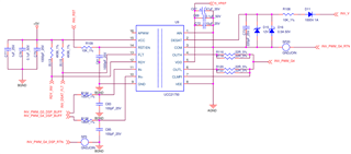
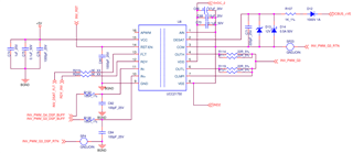
We are test DSAT function on 3 phase VSI using UCC21750.
Condition#1:
When upper switch pulse and lower switch short circuited.
Pulse off time for upper switch is around 1.338us and DSAT FLT report time around 300ns.

Upper switch VCE (C4 Green Color) [Inverter G3 PWM return tied with output V terminal]
DSAT FLT (Yellow Color)

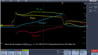
Condition#2:
While lower switch pulse and upper short circuited. Pulse off time 2.184us and DSAT FLT report time again 300ns.
For Lower switch
Lower switch VCE (C4 Green Color) [Inverter G4 PWM return tied with output DC bus -ve]
DSAT FLT (Yellow Color)

I used 100pf as CBLK . and calculated tBLK time is around 1.8us. if we add “leading edge blank time” tDESATLEB around 200ns and tDESATOFF (“DESAT propagation delay to OUT(L) 90% time”) ~300ns. then total time required around 2.3us.
But my upper switch low pulse within 1.338us.
Please guide us why we get two different times.