This thread has been locked.

If you have a related question, please click the "Ask a related question" button in the top right corner. The newly created question will be automatically linked to this question.

LMR16030: WebBench Tina schematic exported has odd passive values

Guru 55913 points
Part Number: LMR16030
Other Parts Discussed in Thread: LM317, LMR36510

Hello,

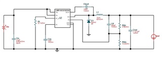
It seems odd that the algorithm to buck +48v down to +24v produced odd component values. Such as the schematic output capacitor is very low (100nF) and 3mΩ FB circuit and BOM used huge 0603 resistors that are not in the NFET switching path, why? The choices that came up for low parts count selection and wide input voltage range for web page to ever show LMR16030 required buck 54v MAX 24v/3A, some selections had over 27 passives though less than 4 is more typical of other bucks, Web bench shows 11 piece BOM. Reference datasheet (SNVSAH9B – DECEMBER 2015 – REVISED MARCH 2021) 

The battery input range +36v - +56v absolute max. Desiging for 48v LiFePo or SLA battery to float 52v max ever rebalancing discussed some forums some batteries refuse to charge though many cycles being left. The actual host PCB current is <1A powered by linear 24v DC supply LM317. The PCB sports 3 Rohm bucks absolute 45v input, hence the reason to update design to handle 48v variable input range. Could you please point me to any other bucks that have fewer passives perhaps specifically designed to handle variable +48v battery source? Why does the schematic for Tina export have only 100nF to hold down switching ripple? The 3 bucks (+5,+12,+15v)  have 22µF ceramic each and one or several distant 22µF bulk electrolytics near current source points. The 3 bucks switch 1.5MHz in 20-40KHZ PWM inductive drive system. Each buck has 9-piece BOM with one EN detect threshold circuit for +5v, +15v, hence SS feature LMR was chosen. The current inductors are 10µH keeping BOM light so LMR 22µH with 1nF output filter seems way off even for 500KHz switching. 

Web Bench exported zip:

/cfs-file/__key/communityserver-discussions-components-files/196/WBDesignSimulation_5F00_LMR16030S.zip   

Thanks for any answers or other devices to meet the requirement!

  • Hello

    The device you selected is a non-synchronous converter that requires an external diode; so that is one extra component.

    The output voltage is 24V, so you need feedback dividers and a Cff. 

    The device has adjustable switching frequency, so you need an extra resistor to set the frequency.

    I am not sure why you are getting strange values from Webench.

    I have attached a design using the LMR16030 from Webench.  The values seem reasonable to me.

    I have also attached a design using the LMR36510 that requires fewer components.

    Of course, TI has other 60V devices that may also meet your needs.

    I hope this helps.

    Thanks

    WBDesign652.pdfWBDesign653.pdf

  • Hi Frank,

    Oddly after lowering the output current several values and frequency changed. The thing that troubles me most is the frequency that came up in the next WB 1.08MHz and 71.1 custom output capacitor is deal breaker. Concern of 1.08MHz being lower than 3 Rhom (1.5MHz) is BFO oscillations in the Bode plot crossover frequency (104KHz) in a closed loop was determined with no other PCB buck devices. 

    Would it make more sense to run any LMR 1.5MHz?  Had not originally read datasheet to find 2.2MHz capable of LMR16030S WB first try (500KHz) for 3A current drive. Why would any LMR not have broad range current WB selected parts to support peak where current limiting is the constraint? That is how the Rhoms behave switching up to 750mA-1A peak with thermal and current limiting 1.2A internal NFET though designed for average 500mA. Have run +12v buck with Nidec fan sources 750mA 16KRPM peak have not had any issues with current limiting.

    Below schematic was for 2.8A 108MHz 34v-54v input. I choose output cap 100µF where Wurth 12µH 2.8A coil saturates 3.5A. Seemingly could handle 1.5MHz tested up to 100MHz, at 1.5MHz looks like 95Ω impedance 216mΩ resistance. Do you see any issue 75-100µF Ecap or stack 4x 22µF/35v ceramic and can the frequency be set to 1.5MHz achieve same current range? Thank you for your interest and fast response.

     WB_LMR16030S_OperatingValues_1.08MHZ.csv

  • The actual host PCB current is <1A powered by linear 24v DC supply LM317.

    That was assumed but review TI-LM317T can source 1.5A with heat sink as it is now configured. I'd like to design LMR for peak 2.5A 1.5MHz so there is additional head room on 24v output rail. Note each Rhom buck now shares 24v input rail with 4.7µF/50v(1206) ceramic and sourced 4.7µF/35V(0805) for LMR 24v output rail and 4.7µF/100V for LMR input. The LMR footprint is considerably large due to Wurth 2.8A coil size so there are some tradeoffs, frequency may be one of them.

  • Hello

    I think that 4x22uF ceramic is best.  With the Ecap you will need to be concerned with the ESR

    affecting the loop response.

    Thanks

  • I'd like to design LMR for peak 2.5A 1.5MHz

    Is the frequency setting pin more about efficiency or peak current capability? The datasheet does not elaborate on why any of the PWM frequency ranges derates efficiency of NFET or package power dissipation curve. The Rohm switchers are fixed frequency, range 1.2 -1.5MHz. So actually a bit variable in the oscillator control loop. Is there a way to get Webench to set the frequency of LMR to prove out various designs?

    From data sheet: The LMR16030 employs fixed-frequency peak current mode control. A voltage feedback loop is used to get accurate DC voltage regulation by adjusting the peak current command based on voltage offset. The peak inductor current is sensed from the high-side switch and compared to the peak current to control the ON time of the high-side switch. The voltage feedback loop is internally compensated, which allows for fewer external components, makes it easy to design, and provides stable operation with almost any combination of output capacitors. The regulator operates with fixed switching frequency at normal load condition. At very light load, the LMR16030 operates in sleep mode to maintain high efficiency and the switching frequency decreases with reduced load current.

    All the LMR sheet graphs are 5v out 500KHz frequency so there is no evaluation at all of the 200KHz - 2.5MHz frequency range. Seems the Webench analysis is the only way to show peak efficiency versus switching frequency. Your 1A 500KHz graphs posted above were very informative. 

  • Hello

    It looks like 1.5MHz would cause too much power dissipation, according to Webench.

    If you need the 1.5MHz, you may want to look into a synchronous converter.

    The choice of frequency depends on many factors.  Higher frequency allows a smaller 

    inductor, both in value and physical size, but results in lower efficiency and more heat dissipation.

    EMI is also a concern with some frequency bands, and their harmonics.

    Thanks

  • It looks like 1.5MHz would cause too much power dissipation, according to Webench.

    Oddly Webench came up with 1.08MHz so we will go with that frequency. The thermal pad is the larger outline with 8x TH via though top & bottom pads have clearance with a surround opening. Does the LMR thermal pad require specific size copper area to dissipate 1.08MHz? The LMR may never peak 2.5A though head room exists for inrush ect...

  • Checking the cvx file it was 1.08MHz for 1A but I put in 2.5A for the analysis. A recheck design Webench shows 763.76KHz now 2.5A. Oddly the value sliders blue tear drop are being covered by title bar (Edge browser) makes it difficult to read and change slider values.

  • Hello

    You can use the graph below to estimate the required copper area required

    for a given thetaJA; it is only approximate.  We usually specify 4-layers, 2oz on outside and 1oz on inside.

    Thanks

  • Hi Frank,

    What graph below?

    It's two-sided 2oz PCB with digital GND top/bottom, isolation high voltage ground via 0R copper zones. Multilayer PCB often have future via issues can't withstand high surface temperatures even 2oz warpage is sure to occur. Notice many TI 4-layer launch pads have some amount of warpage, hence my fear and added cost choose to use other counter measures. Such as via placement joining top to bottom around zone flood fills component thermals to ground, KiCad has amazing zone priority control. 

  • Hello

    Here is the graph.

    Thanks

  • I really do not get how 4-layer PCB has anything to do with HSOIC package as thermal pad and vias should be isolated from any middle layers. Surely the above graph is not Cm^2 that would be huge square inches most any PCB would not have that kind of free space. Note Fig.10-1 shows small copper space for the thermal pad, not much more. For example, 30cm equals 11.8" of copper. Seemingly 30mm^2 equals 1.81" copper a bit more believable. 

    I modified the broken Tina analysis with actual component values, 48v input supply block only bucks to 18.5v after 38 minutes of transient analysis. Yet even that analysis model is missing the thermal pad power dissipation. The analysis model graphs show seconds but it's more like minutes for some odd reason. The model uses encrypted LMR chip custom parts that take forever to run on quad core Intel CPU 2.8GHz. Oddly the Tina model shows only 2A diode for 2.5A peak so 3A seems more plausible. A 60V diode should be more efficient than 100V diode as the forward VD typically smaller 60v and again a good MOV should easily stop transients >56v. Most Schottky diodes have absolute maximum blocking voltage, never shown on datasheets as peak blocking voltage.

    https://webench.ti.com/power-designer/switching-regulator/export/19

  • Hello

    The thermal vias must be connected to all ground layers under the device to provide

    the most effective heat sinking.  Although the inner layers are not as effective as the outer layers,

    they do provide some heat sinking.

    Thanks

  • Not recommended to do that by any PCB manufacturer as the layers bonding agent will expand slower than under layer copper warping layers. On the other hand, glueing an aluminum finned heat sink to the underside copper island surrounding thermal pad outline would be an exceptional thermal control design technique and keep LMR thermal dissipation away from other devices. The question is how big AL heat sink being centimeters squared seems very odd indeed and next LMR design should invert the heat pad top side as to isolate thermal dissipation upward and away.

  • next LMR design should invert the heat pad top side as to isolate thermal dissipation upward and away.

    Thanks for your advice, it is very inspiring to next generation.

    B R

    Colin

  • Hi Frank,

    That Fig.22 above you never answered my question about centimeters versus millimeters. The total Pd is only 3.2 watts +24v 2.5A linear output current not average current. Yet LMR drive feeds 3 downstream bucks sourcing average current drawn via 85µF output reservoir capacitors. Even if required minimum 10Cm^2 copper that would be a huge area for Pd of only 3.2 Watts. It's not like heat pad is dissipating even 10 watts. Given the graph curve hypothetical for theta resistance pad to foil 34°C/W the NFET junction would be near 109°C. So 10cm^sq (10x10=100cm foil area) 39.37" of foil for 3.2 watts, really? Seems the graph is for some other device not LMR has absolute MAX 150°C. LMR can't be 94% efficient and generate that kind of junction heat, wasted energy!

    LMR datasheet shows RθJB Junction-to-board thermal resistance 25.5 °C/W through metal pad to copper PCB area. That is excessively high thermal resistance to heat transfer, e.g. NFET substrate + epoxy + metal pad to PCB copper. For example we use a silicon heat pad rated 16W/°C resistance on TO220 NFETS that can run at 175°C. So I have hard time believing 45cm^2 foil required at 25.5°C/W thermal resistance heat transfer. 

    RθJC(bot) Junction-to-case (bottom) thermal resistance 3.8 °C/W is more likely the thermal pad resistance, not the case.

  • Hello Sir,

    I will go through your comments and update with next week.

    Colin

  • Some of the issue is the Tja and RθJC(bot) data sheets package design assume 2D space, top view is front, bottom is back in 3D CAD space. Looking at LM317KCS package is 2D model for 3D part being very confusing. So TO220 does not mount bottom tab to PCB and top = front and bottom = back. Need to note 2D or 3D CAD space describing SMT thermal pad and vertical placed components are 3D, not 2D CAD view, accept footprints. Always package legs being very high thermal resistance when it comes to bottom metal plate epoxy substrates carry the main Tja to copper foil or ambient air.

    LM317KCS:

    RθJC(top) Junction-to-case (2D top) thermal resistance 43.2 (3D Front) 15.9°C/W

    RθJC(bot) Junction-to-case (2D bottom) thermal resistance (3D back) NA 0.1 °C/W

    LMR datasheet shows RθJB Junction-to-board thermal resistance 25.5 °C/W through metal pad to copper PCB area

    WB_LMR16030S_OperatingValues_760KHz.csv

    So 94% LMR buck efficiency the input drop 48v to 24v produces very little IR for 2.5A load, Pd = 3.2 watts. Perhaps the decimal point is in the wrong place RθJB Junction-to-board thermal resistance? That is terrible thermal resistance for device rated 3A claims high 90% efficiency.  

  • Hello Genatco,

    LM317KCS has different package like SOT 223 and TO220.

    You can see for SOT223, the RθJB has reached to 16.8°C/W as well.

    So I think it is normal to have RθJB=25.5 °C/W for LMR16030 because of bigger package size (SOIC 23-6).

    You can refer  more to below link: https://www.ti.com/lit/an/spra953c/spra953c.pdf?ts=1708306922270


    B R

    Colin

  • Nobody has that kind of test setup unless they are TI engineers laboratory. Again RθJC(bot) Junction-to-case (2D bottom) thermal resistance (3D back) NA 0.1 °C/W is more realistically TO220 metal tab thermal contact resistance, not the junction to case. Otherwise the junction would exceed °C for only a few watts of dissipation via simple math. Tina analysis wattage probes on LM317 seems to agree the ѱJB value LMR datasheet is not common outside the cold plate experiment since junction to board includes the thermal metal plate embedded in the case.

    Also discovered LMR16030sdda_trans.olb Cadence model with wattage probe placed inside Spice block does produce a thermal graph. Oddly the pulse peaks seem to push upward 100 watts for <3A load. The input and load currents plot as negative graph values and much greater than 3.35 watts listed in Webench CSV file. 

  • Hi Sir,

    I am not sure this model can test power directly.

    I see Vout can be 30V and Ioad<3A,so the peak power can be 100 watts.

    Thanks

    Colin

  • If the device package is also dissipating Tja (42°C) the peaks can never reach 100 watts. The analysis seems wrong sustained peaks of 100 watts would eventually burn the FR4 PCB even in direct contact with copper foil. One purpose to run Pspice simulation is also to determine how much foil is required to dissipate peak wattage from Tja peak.

    Oddly the current and watt probes cannot be added to a plotted graphs though present in the macro when simulation probes are removed. Similar probes added to Tina LMC317KCS circuit has excellent DC analysis of input to output power. Oddly same probes placed on Tina LMR macro produce no DC analysis input or output load.

    Cadence steady state LMR16030 is not producing peak power in 350µs. Actually takes 4.5ms to see the peak voltage, current and wattage is not a selection in the output graph trace properties when adding graphs. I copied the modified passives values schematic from transient into steady state analysis and updated the netlist, remained the same in both simulations there was no change in the cache.

    Remain puzzled as to what is happening though steady state plots do produce 4 graphs. Also removing SS pin capacitor from the schematic did not seem to matter and LMR macro SS = 1 still requires 4.5ms to reach full voltage current load.  

    The load is only 2.5A regulates 24v out FB loop to produce 60 watts maximum.

  • Hello Genatco,

    Sorry Sir, for LMC317KCS it don't belong to us  and  you can ask other product line for better support.

    Many Thanks

    Colin

  • The LM317KCS datasheet is TI part, C was a mistake. Anyway the LMR16030S steady state Spice model peak voltage exceeds 27v out when zoomed in at the end of the graph. The Webench Pspice FB loop sense resistors are to maintain roughly 23.99v output for 48v input. Might this be a transient analysis error?