Because of the holidays, TI E2E™ design support forum responses will be delayed from Dec. 25 through Jan. 2. Thank you for your patience.

This thread has been locked.

If you have a related question, please click the "Ask a related question" button in the top right corner. The newly created question will be automatically linked to this question.

BQ25155:EVM_Board BQ25155EVM & EV2400

Part Number: BQ25155
Other Parts Discussed in Thread: EV2400, , BQ25150

We have started considering evaluation boards.
It seems like the assumption is that VDD output = VIO input is used as the default.
Personally, I tried connecting it to use VLDO output as VIO input.
I am experiencing a problem. Could you please tell me how to resolve it?
Thank you for your support.

VDD output = VIO input
5V input from USB connector to BQ25155EVM board
VDD output = VIO input VIO is 1.8V.
Connect EV2400.  VIO is 1.8V.


VLDO output = VIO input
5V input from USB connector to BQ25155EVM board
VLDO output = VIO input VIO is 1.8V.
Connect EV2400.  VIO is 3V.
  ↑Why is this?

  • Hi,

    To clarify, VLDO in this case is the LDO that is present on the BQ25155EVM?

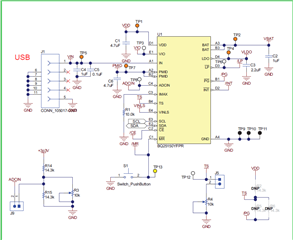
    The EV2400 has internal I2C pull-ups up to 3 volts so it is likely that the voltage is being backfed to VIO via the pull up resistors. Try disconnecting J17, the EV2400's pull up resistors should still allow I2C Transactions.

    Best Regards,

    Juan Ospina

  • This is the LDO output of pin D4 in the attached EVM circuit diagram.

    I can guess that this is due to the internal pull-up of the EV2400's I2C line.
    However, if the supply voltage to VIO is connected to VDD, which is the same 1.8V, it is unaffected.
    Why is VLDO's 1.8V affected?

  • P.S.

    Idon't know what happens with the EV2400's I2C line pull-up, but if it is pulled up at 3V etc. and the VIO voltage is 1.8V, wouldn't a reverse voltage be applied to the BQ25155 chip?

  • Hi,

    I'm not entirely sure of the cause. I can try to recreate it on my EVM, but this may relate to the internal impedance of VDD vs VLDO. VLDO is meant to handle larger loads so it can more easily compete with the EV2400 pull up rail.

    Best Regards.

    Juan Ospina

  • You say you don't know the answer, but that's a problem because you won't be able to confirm using the evaluation board.
    Please investigate the cause.

    I got the EV2400 circuit diagram from the internet.
    When I checked, it seems to be a circuit that can change the voltage of the PullUp resistor.

    Isn't it possible to change it from the PC application that controls the EV2400?

    I want to operate VIO by connecting from VLDO output,
    Could you please think of a solution?

    Also, the VIO voltage is selected between 3.3V or VDD1.8V on the evaluation board, but how is the EV2400's I2C control pull-up voltage controlled?

  • Hi,

    You should be able to disconnect the VIO from the EV2400 by removing jumper J17. If you remove this jumper and you still see 3V on VIO then this may indicate part damage.

    Does that resolve the 3V issue?

    Best Regards,

    Juan Ospina

  • By open J17, operation became possible.
    Thank you.
    My question is, does this mean that there is no problem whether the SCL/SCK voltage is high or low regardless of the VIO voltage?
    In this case, the VIO voltage is 1.8V or 3.0V and the SCL/SCK voltage is 3.3V, but is it correct to understand that the port voltage will not flow backwards inside the BQ25150/BQ25155 and cause any problems. ?
    Also, on the other hand, even if the VIO voltage is 3.0V, is there no problem if the SCL/SCK voltage is 1.8V?
    I don't understand the specifications of the chip, so please let me know.

  • P.S.
    Regarding the VIO voltage, do you mean setting the output voltage of the IO port voltage of the BQ2515ⅹ chip?
    Is the IO port input 5V? Is it correct to assume that the level is shifted to the VIO voltage inside the chip without any problems?

  • Hi,

    My question is, does this mean that there is no problem whether the SCL/SCK voltage is high or low regardless of the VIO voltage?

    There is no issue if the I2C pull-up voltage is higher than VIO. If it is lower then there may be communication difficulties.

    In this case, the VIO voltage is 1.8V or 3.0V and the SCL/SCK voltage is 3.3V, but is it correct to understand that the port voltage will not flow backwards inside the BQ25150/BQ25155 and cause any problems. ?

    No, a higher I2C Pull-up voltage should not flow backwards to cause issue.

    Also, on the other hand, even if the VIO voltage is 3.0V, is there no problem if the SCL/SCK voltage is 1.8V?

    This may be a problem since VIO is expecting close to 3.0V for a high voltage detection. I2C can be higher but we don't recommend that it be lower than VIO.

    Best Regards,

    Juan Ospina

  • do you mean setting the output voltage of the IO port voltage of the BQ2515ⅹ chip?

    Can you please clarify what you are referring to? The device's digital input output voltages is set by whatever rail is connected to VIO. Typically this is connected to VDD. It is designed to level-shift the IO voltage without any issues.

    Best Regards,

    Juan Ospina


  •                  ↑The red frame block circuit above is connected to VIO.

    The inputs of CE/SCL/SCK/LP/MR are configured with a level shift, so there is no problem even if the input voltage is higher than VIO.

    Is the above understanding correct?

  • Hi,

    With regards to connections directly to VIO, this should be limited to an upper limit of 3.6V per the Recommended Operating Conditions:

    With regards to CE/SCL/SCK/LP, a higher voltage than VIO can be placed on these pins without issue as long as it is not above 5.5V per the Absolute Maximum Ratings:

    For the MR pin, this pin has an internal pull up resistor to BAT of 125 kOhms. Placing a voltage on this pin that is higher than the battery voltage can cause unexpected current into the battery. We usually do not recommend applying voltage to MR, just pulling it down when signaling to this pin.

    Best Regards,

    Juan Ospina