This thread has been locked.

If you have a related question, please click the "Ask a related question" button in the top right corner. The newly created question will be automatically linked to this question.

TPS568230: Regulator's output ramps even if Enable is not provided & VCC ouput supply has ripples.

Part Number: TPS568230

Hi Ti Team,

I have used multiple TPS568230RJER devices in our projects. 

We are facing couple of issues with this module, please go through the following problem statement- 

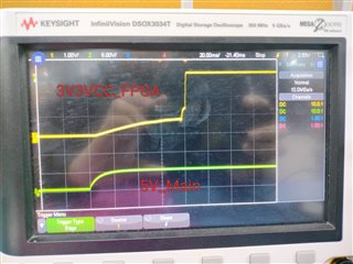
Problem- 1: Regulator's output voltage ramps even if Enable is not provided.

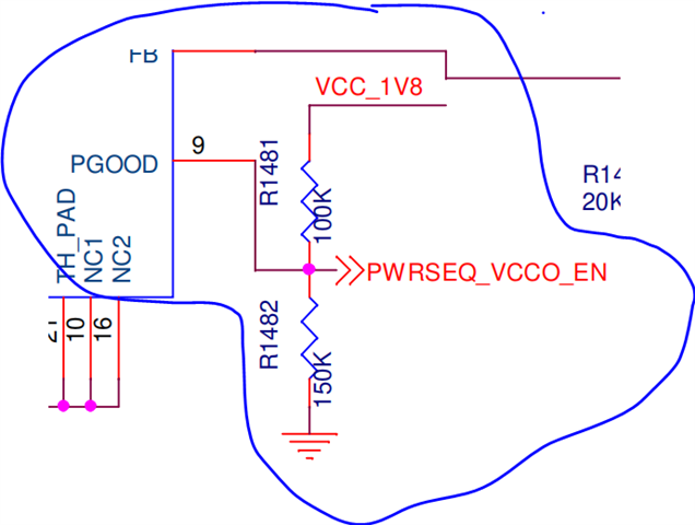
Actually, we are deriving FPGA's supply like (1V, 1.8V, 1.5V, 3,3V, etc) using the same device (TPS568230RJER). Enable and power goods of these devices are connected to implement the desired power sequencing.

Here we will talk about only the 3.3V regulator whose enable pin is driven by power good of 1.8V regulator. But, This 3.3V regulator's output voltage starts ramping around 40-60ms before getting its enable signals from 1.8V regulator. this ramp voltage reaches up to 0.9V from 0V during this 40-60ms duration.

for your reference, please find the snaps of corresponding schematic-

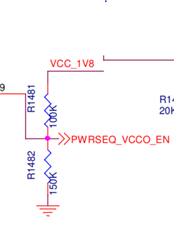
As Enable pin doesn't take voltage above 3.6V so voltage divider circuit is applied on power good of 1.8V (between VCC and ground).

3V3 regulator's output waveform can be seen in the following image-

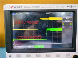
Problem-2: When I probed the VCC pin of the regulator which is ouput pin of internal LDO. I observed the ripples, please refer the following image-

Please look into this as soon as possible, as we are facing the issue in debugging and the same part number is used for other ongoing projects also.

Thank You 

Raj Kumar

  • Hi Raj,


    For Q1.

    Can you provide the Enable signal waveform for3.3V regulator  and

    also how is the PGood of the previous stage pulled to and can you provide the PGood wave form for the same 

    For Q2

    Can you actually provide the VCC waveform directly across the VCC cap, are the wave forms provided by you are of PGood ?

    and what is the Vcc cap and rating of those caps?

    Can you take the forms with tip and barrel method at with a proper ground and limit your Band width to 20MHz.

    Thankyou

    Savith

  • Hi Raj

    Do we have any update on this request

    Thank you

    Savith

  • Hi,

    For Q1.

    I have already shared the image (under problem-2). VCC1V8 PGOOD signal is the Enable of 3V3 regulator.

    A voltage divider between VCC & GND is implemented on Power good of previous stage (see image-)

    For Q2:

    The VCC waveform is not directly probed across the Dcap on VCC.

    The given waveform was of Power Good (which is pulled up to VCC).

    The Dcap ratings are- 1uF/ 16V/ 0603/ X7R/ 10%

    Thank You 

    Raj Kumar

  • Hi Raj

    Based the information provided i cannot answer completely,

    1. looking at 5V VCC waveform it looks clean, but the traces maybe picking up noise (not sure if it is your layout or the way you are measuring)

    2. Can you provide the EN waveform, so that we can compare it to threshold levels 

    3. what are the measurement techniques you are using and where are you probing on your board

    it would be useful if you can provide the layout file

    Thank you

    Savith

  • Hi Raj

    Any update on this ?

    and I am closing this and feel free to reopen for further assistance

    Thank you

    Savith