This thread has been locked.

If you have a related question, please click the "Ask a related question" button in the top right corner. The newly created question will be automatically linked to this question.

TPS65219: TPS6521902RHBR after press "PB" still no output power.

Part Number: TPS65219

Hi all,

My product need PB with short press and long press function and 2 output power.

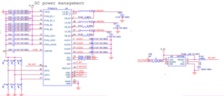
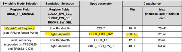
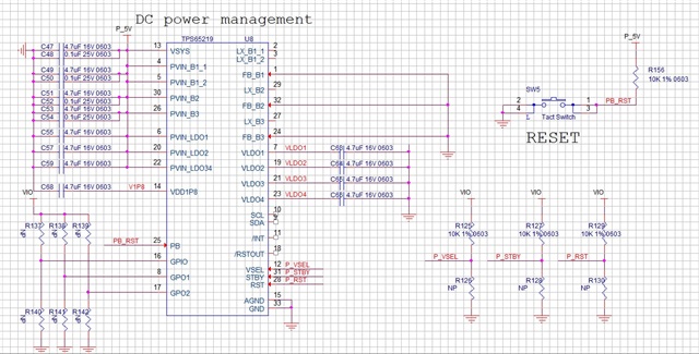
I select TPS6521902RHBR  to fulfill my product.


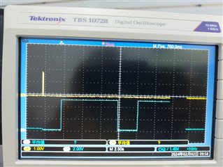
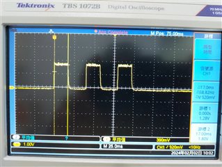
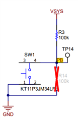
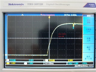
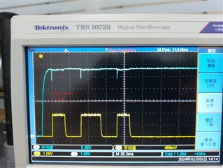
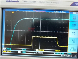
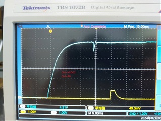
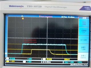
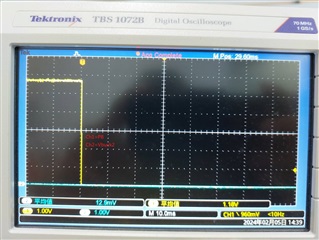
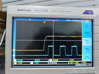
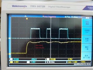
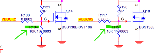
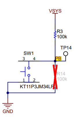
When I get ICs, in order to test "PB" function. Below is my test circuit.

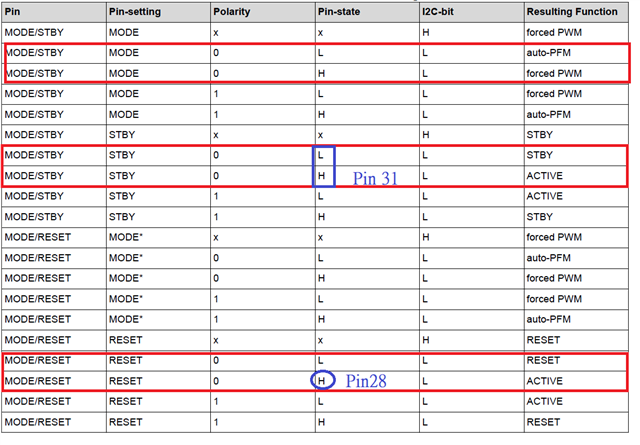
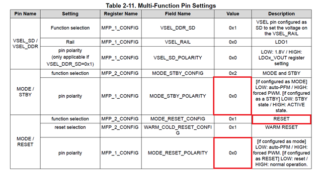
I try to use different kind of configure for VSEL/STBY/RST (pin12/pin31/pin28), but after press "PB" (pin25) still no output power.

Please help to help my questions as below:

Question 1: Plese help to checck if my circuit is NG or need to modify?

Question 2: Does  TPS6521902RHBR need MCU to commuate to set output voltage?

Question 3 : Does  TPS6521902RHBR can work normaly without MCU? How to do it? 

Please provide help.

Thanks

Best Regarfds,

Eric

  • Hi,

    Thanks for reaching out! What processor or SoC are you powering with the TPS65219 PMIC? TPS6521902 is a pre-configured device that was programmed to meet the power requirements of the Sitara AM62/AM64 processors. This device has all the power rails (Bucks and LDOs) enabled by default so they should all have the required external passive components. Your schematic is missing a lot of components specially the inductor and output capacitor for Buck1/2/3.

    If you would like to evaluate a custom NVM configuration, we recommend using TPS6521905 which is the user-programmable version. This variant can be easily programmed to have specific rails disabled by default so you don't have to add the external components for the rails that are unused. Here is the collateral available. Let us know if you have any questions or need assistance with the programming process. 

    Thanks,

    Brenda

  • Hi Brenda,

    Thanks for your reply.

    We use this chip because we need "short press" and "long press" pusb-buttom function. And maybe one or two LDO output voltage.

    That's why I don't need buck voltage. As below datasheet . All buck if not used, feedback connect to GND and LX_B1~LX_B3 leave floating.

    That's why my schematic missing a lot of component.

    My requirement is when short press , one LDO output voltage turn on.

    And when long press, one LDO or all power turn off.

    Please help to provide your suggestion.

    Thanks

    BRs,

    Eric

  • Hi,

    The column "Connection if not used" is applicable for rails that are disabled by default in the NVM configuration. TPS6521902 has all rails enabled by default even though some of them are not used in your schematic.  

    We can help to create a custom NVM configuration file with the Bucks disabled by default. This file can be used along with the programming board and the GUI to re-program the PMIC.  

    Thanks,

    Brenda

  • Hi,Brenda,

    If buck converter relate component not in the circuit. Will it make LDO output NG?


    If buck converter relate component missing and make "NO" buck output voltage , I can understand it.

    But if buck converter relate component missing and make "NO" LDO output voltage, I can't understand why.

    Please help to provide your suggestion.

    Thanks

    BRs,

    Eric

  • Hi,

    The reason is because the TPS6521902 PMIC monitors all output rails that are enabled by default and if a fault is detected, the power-up sequence is aborted. This is a typical behavior of a PMIC. During the power-up sequence, if a rail doesn't reach the UV (under-voltage) threshold, the next rail in sequence does not get enabled. 


    Thanks,

    Brenda

  • Hi Brenda,

    Thanks for your reply. I will check buck voltage relate component.

    I still have some question about Pin12/ Pin28 / Pin31

    Because our chip is tps6521902. Please refer to below table.

    Suppose Pin28 and Pin 31 should set high level voltage. Am I right?

    How about Pin 12? Should I set it high level or low level? Why?

    Please help to provide your suggestion.

    Thanks

    Best Regards,

    Eric

  • Each orderable part number has a Technical Reference Manual (TRM) that describes the default register settings. Pin# 12/28/21 are the digital multi-function pins and they are configured as described below. If you dont have a processor/SoC driving those pins, I recommend having a pull-up resistor on MODE/STBY and MODE/RESET. VSEL must have a pull-down resistor (to GND). We also recommend reviewing the output capacitance requirements in the data sheet before finalizing the next schematic revision. All LDOs use a typical 2.2uF output capacitance (after de-rating).

    • MODE/STBY
      • LOW: PMIC in Standby state and Bucks operate in auto-PFM.
      • HIGH: PMIC in Active state and Bucks operate in forced-PWM.

    • MODE/RESET
      • Falling edge: PMIC triggers a warm reset (all register settings go back to the default values)
      • High: Normal operation

    • VSEL:
      • Low: VLDO1 in "LDO-mode" with output voltage=1.8V
      • High: VLDO1 in "Bypass-mode" with output voltage=3.3V (requires PVIN_LDO1 = 3.3V)

    Thanks,

    Brenda

  • Hi Brenda,

    Below is my update schematic.

    I already add all component to relate buck converter and add pull high or pull low resistor to pin12/pin28/pin31 as your suggestion.

    But when I test it still NG.

    Please see below photo.

    Ch1 (Yellow color) =Vbuck2

    Ch2 (Blue color) =PB_RST

    when power on, Vbuvk turn on for 3 times then off. 

    PB_RST pull H after a period time due to U9 (Delay IC)

    But when PB_RST from High to Low, Vbuck2 do not have any response or different.

    Does TPS65219 need to set by I2C when power on?

    Do you have any suggestion about it?

    Thanks

    BRs,

    Eric


  • Hi,

    What is the delay from U9 (PB_RST)? The EN/PB/VSENSE pin of the TPS6521902 is configured as "push-button" with FSD (first supply detection) enabled. This means the PMIC ignores the state of the PB pin during the first power-up (until nRSTOUT is released). Once the PMIC finishes the power-up sequence, it starts monitoring the PB pin and if it is low, the PMIC executes a power-down sequence transitioning to Initialize state.

    Here are the potential root cause of the issue: 

    • long delay of external signal driving the PB pin. 
    • slow ramp on the pre-regulator (P_5V). See more details on page#10 of the following Apps note: https://www.ti.com/lit/pdf/slvafd0

    Could you remove U9, keep a pull-up resistor on PB_RST and let us know if the PMIC is able to finish the power-up sequence? We would like to see a power-up capture (with ~4ms time scale) showing the voltage on VSYS (P_5V), PB (PB_RST), Buck2, VLDO2. 

    Thanks,

    Brenda  

  • Hi Brenda,

    Please refer to below.

    1. I have remove U9 and make PB as same circuit as below.

    2. Power sequence as below. 

    2.1 VSYS and PB

    2.2 PB and Vbuck2

    2.3 PB and Vbuck2

    2.4 PB and VLDO2

    2.5 Vbuck2 and VLDO2

    2.6 Press PB and Vbuck2

    For Vbuck and LDOs. I only connect Vbuck2 to VIO for pull high STBY and RST (Pin 31 and Pin28)

    No any other output voltage connect to device.

    My circuit almost the same with EVB circuit. (Except MCU)

    But still no output power .

    Please help to provide your suggestion.

    Thanks

    BRs,

    Eric

  • Hi Brenda,

    Additional waveform:

    Befor Vbuck2 connect to VIO. And I try to disconnect from Vbuck2 to VIO and provide VIO power by power supply.

    After that, PB do not have dropout voltage .(Please refer to below)

    I try to check any possible to make no power ,but still find nothing.

    That's why I am curious if this chip need to setup by I2C befor initialize.

    And some question need your help.

    1. Do I need to provide pull high voltage to I2C ?

    2. What shall I do for GPIO/ GPO1/ GPO2/ /INT/ /RSTOUT(Pin 16/ Pin8/ Pin17/ Pin11/ Pin18)

        These are output signal, and I let all of these floating. Will it possible to make no power?


    Please notice that I send "2" reply. Please  check the "2" reply and provide your suggestion.

    Thanks

    Best Regards,

    Eric

  • Hi,

    Thanks for sharing the scope captures. LDO2 is the last rail to turn-ON in the TPS6521902 NVM cnfig. It seems like the PMIC is able to turn ON this LDO for approximately 1ms until a fault is detected. Here are my comments and suggestions for the next actions:

    • The max operating voltage for VSYS (PMIC input supply) is 5.5V. The scope captures show VSYS operating at the edge or beyond spec. Could you lower the input supply to 5V?
    • GPIO/ GPO1/ GPO2/ /INT/ /RSTOUT are all open-drain outputs. You dont have to add an external pull-up if they are unused in the application.
    • We recommend to use nRSTOUT in the actual application. This pin can act as a power-good signal indicating the PMIC has completed the power-up sequence. 
    • I2C communication (SCL/SDA) is not required to execute the power-up sequence. 
    • Could you share the layout? 
    • Could you share the latest schematic? showing all the pull-up or pull-down resistors for the digital pins? 

    Thanks,

    Brenda

  • Hi Brenda,

    I add layout and schematic as attach file.

    Please notice that, when I test. I remove R144 and connect  net: PB_RST to Ext_Press

    Vbuck1: No connect to device

    Vbuck2: Connect to two PMOS and VIO and purge pump(Note: Do not mount 0ohm resister from Vbuck2 to purge pump)

    Vbuck3: No connect to device

    VLDO1: Connect to VIO and purge pump and I2C source(Note: Do not mount 0ohm resister from VLDO1 to VIO and VLDO1 to purge pump)

    VLDO2: No connect to device

    VLDO3: No connect to device

    VLDO4: Connect to VIO (Note: Do not mount 0ohm resister from VLDO4 to VIO )

    Please help to check attach file and provide your suggestion.

    Thanks

    Best Regards,

    Eric

    To-TI_0206.brdTO_TI.DSN   

  • Hi Brenda,

    One more question . We are curious that PB belong to "ON-Request", but it should be "Low" level to be On-Request.

    Please refer to below photo. In this photo, PB was high level.(Not yet press PB button) 

    It should not be a "ON-Request", but vbuck2 output already turn on then off.

    Does it's normal or abnormal?

    Please help to clearify it and provide your suggestion.

    Thanks.

    Best Regards,

    Eric

  • Hi,

    The TPS6521902 does not require an ON request to execute the first power-up sequence. This NVM has the enable pin configured as "push-button" with FSD (First Supply Detection) enabled. This means the state of the EN/PB/VSENSE pin is ignored during the first power-up (until nRSTOUT is released).

    Could you share the schematic in PDF? Could you also lower the input supply to 5V and disconnect any load from the PMIC rails?  

    Thanks,

    Brenda

  • Hi Brenda,

    I have remove all load. And provide VIO power by power supply.

    Below is VSYS and Vbuck2 still no power.

    Schematic by PDF as attach file.

    Please help to analysis root cause and provide your suggestion.

    Thanks

    Best Regards,

    Eric

    To-TI_0206.pdf

  • Hi,

    Thanks for sharing the schematic in PDF. We will review it and provide an update within 24Hrs.

    Thanks,

    Brenda

  • Hi Brenda,

    Thanks for your review and waiting for your reply & suggestion.

    Thanks,

    Best Regards,

    Eric

  • Hi,

    Thanks for your patience! I have added my feedback below. The information in the first three bullets is critical for the PMIC operation. Let us know if there are any questions. 

    • The required Bucks output capacitance depends on the configured switching mode. TPS6521902 was configured as Quasi-fixed frequency and high bandwidth. This mode requires a minimum of 30uF local capacitance (after de-rating). 47uF per Buck is typically used. Here is a capture from the data sheet:

      • Are ALL loads disconnected from the PMIC output rails? Please disconnect any load from Buck2, including external pull-don resistors like the ones highlighted below. 

    • How are you driving the PMIC PB pin (R14PB_RST)? It is recommended to have an external pull-up to VSYS on this pin. As noted in the data sheet, the voltage on the PB pin must not exceed the voltage on VSYS at any time. The PB pin has an internal low resistance to ground that could pull a lot of current from the supply. Could you add a 100k Ohms pull-up to VSYS (P_5V) on the PB pin?

    • VDD1P8 uses a typical 2.2uF cap

    • All LDOs (VLDO1, VLDO2, VLDO3, VLDO4) use a typical 2.2uF.

    Thanks,

    Brenda

  • Hi Brenda,

    Thanks for your suggestion.

    1. I will add capacitor more than 30uF for all Buck output voltage.(Vbuck1 / Vbuck2 / Vbuck3)

    2.For VDD1P8 uses 4.7uF now. Do I need to decrease it to 2.2uF?

    3.All LDOs (VLDO1, VLDO2, VLDO3, VLDO4) use 4.7uF now. Do I need to decrease it to 2.2uF?

    4. For Below circuit, I already remove R108 and R117.

    5.For PB_RST (Pin25) , I will modify as below circuit with 100K ohm pull high resistor.

    Please help to check if above step is correct.

    And I will do it on 2/15 ( after Chinese new Year).

    Thanks

    Best Regards,

    Eric

  • Hi,

    Yes, those seem to be the same items I had highlighted in my previous message. As noted in the PMIC data sheet 2.2uF is the recommended capacitance for VDD1P8, please update this component if the value in your schematic doesn't match the data sheet.

    Similarly for the output capacitance on the LDOs. As noted in the data sheet 2.2uF is typical and 4uF is the maximum local capacitance. If the local output capacitance in your schematic exceeds 4uF after de-rating, they would have to be reduced. 

    Thanks,

    Brenda

  • Hi Brenda,

    Thanks for your suggestion.

    After add Vbuck output capacitor more than 30uF. Vbuck is ok.

    One more question.

    For our requirement, we want to have Vbuck2 after short press "PB" (Pin25 pull L)

    But Vbuck2 have output voltage when VSYS is ready now.

    Are there any way to make Vbuck2 have output voltage after press "PB" instead of VSYS is ready?

    Please provide your suggestion, thanks

    Best Regards,

    Eric

  • Hi,

    I'm glad to hear our suggestions helped to resolve the issue! Did you confirm all the PMIC rails are turning-ON as expected without any issues?

    Regarding your question about PB: The TPS6521902 has this pin configured as "push-button" with the first supply detection (FSD) enabled. This means the PMIC ignores the state of the PB pin during the first power-up until the sequence is complete (until nRSTOUT is released). The FSD feature can be disabled by changing the "PU_ON_FSD" register field on address 0x20 but all register settings go back to their default values after power-cycle.  

    Please note, we recommend using the TPS6521905 user-programmable version if your application requires changing any of the default settings of a pre-programmed device. The user-programmable PMIC allows to have a custom NVM configuration with unique settings (for example, with the FSD feature disabled by default).  

    Thanks,

    Brenda

  • Hi Brenda,

    Below is all buck and LDO output voltage. I am not sure if Vbuck1 and Vbuck2 are normal or abnormal.

    Please help to check.

    Vbuck1: 0.75V  ;  Vbuck2: 1.8V  ;  Vbuck3: 1.1V

    LDO1: 1.8V  ;  LDO2: 0.85V  ;  LDO3: 1.8V  ;  LDO4: 2.5V

    For FSD and relate question, I will check with my FW colleague.

    Thanks for your great support.

    Best Regards,

    Eric

  • Hi,

    Yes! those are the correct output voltages that were programmed on the TPS6521902 NVM. Just for reference, here is the link to the Technical Reference Manual with the list of the default register settings:  https://www.ti.com/lit/pdf/slvucl0

    Thanks,

    Brenda