This thread has been locked.

If you have a related question, please click the "Ask a related question" button in the top right corner. The newly created question will be automatically linked to this question.

LM25143: Can LM25143 use for power FPGA

Part Number: LM25143
Other Parts Discussed in Thread: UCD90124, LM5143, LM5117

Hi TI expert,

My project is to design PSU circuit for Xilinx FPGA Versal Prime VCCINT, I had study TI reference power solution but that design over my requirement and using too much space.

So I check that the TI part LM25143 may also fulfill my requirement, do this part used for power FPGA before?

Below are my Design Spec

Vin: 12V / 24V

Vout: 0.88V

Iout(max): 40~60A

Vripple +/-2%

Also attaching the quickstart design tool table for you understand the choosen part.

LM(2)5143-Q1 quickstart design tool - revB2_For_Xilinx_Versal_Prime.xlsm

Thanks a lot.

Alex.

  • Hello Alex,

    I checked the file you attached, suggest dropping the switching frequency to 100kHz to help with the temp rise and more importantly to ensure you do not go into duty cycle saturation at Vin max.  this device has a minimum Ton min specification and operating near there can cause poor transient performance.  

    also be sure to set your current limit 10 10 12% above the output current requirement.

    Hope this helps.

    David.

  • Hi David,

    I have change the Fsw to 100kHz and it need some parts change, but that also push the Efficency above 80% most of the current load.

    I think I will mixing some Tan / Polar Cap (22uF*4 +10uF*4 input, 1000uF*2+100uF*4+47uF output) to reduce number of Cap in design.

    By checking the BOM I found the RHO (outside of pin HO1/2) are missing, any suggested value?

    Thanks,

    Alex.

    LM(2)5143-Q1 quickstart design tool - revB2_For_Xilinx_Versal_Prime_TI_reply.xlsm

  • Hello Alex,

    for now, suggest 0hms in the high side gate drive Ho1 and 2, no resistors needed in the low side gate drive. makes sure you place resistors close to the IC and route differentially as instructed in the datasheet.

    Hope this helps.

    David.

  • Hi David,

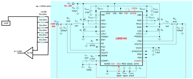
    Here come another question is there any recommandations of measuring the 2-phase current output?

    As this is a 2-phase Buck conventor, reading Vdiff of single sense resistence cannot represent whole system output.

    In my system I am using UCD90124 as Power sequencer, with an embedded 2.5V ADC for current reading.

    So I am thinking of parallel 6pcs 5m ohm and a G=50 current sense Amplifer.

    is it possible? 

    Thanks,

    Alex.

  • Hello Alex,

    You can stack the LM5143 controllers for 6 phase, the only thing you need to account for is clock sequencing to ensure the 6 phase clock timing are evenly over 360 degrees,

    please refer to the 4-phase configuration and stack another device for 6 phases.

    hope this helps.

    David.

  • Hi David,

    May I clerify my question, is there any method I can measure the current output of this system?

    on my system I am using UCD90124 to monitor voltage rails with 2.5V ADC for voltage reading, which can also be use as reading current.

    Thanks,

    Alex.

  • Hello Alex,

    Good place to start, is looking is into using a current sense amplifier, link to our INA amplifiers below, interestingly, we do have an older part, the LM5117 that has a current monitor pin built in.

    Current-sense amplifiers | TI.com

    hope this helps.

    david.

  • Hello David,

    I have one more place need to clarify, From the Excel table, page "BOM&Schematics" it suggest 2 part can be use as N-ch MOSFET in schematic

    "NVMFS5H663NL" and "NVMFS5C628NL"

    Should I use the same part for all MOSFET (e.g. Q1-Q4 = NVMFS5H663NL)

    Or it has to be in order? (e.g. Q1,Q3 = NVMFS5H663NL ; Q2,Q4 = NVMFS5C628NL)

    Thanks,

    Alex.

  • Hello Alex,

    For an optimal effieicnt desgin, suggest going with the 2 types of FETs and not using all 4 of the same.  The reason being is for a high step-down ratio the LS FET is on most of the period.  This will incur the most I^2R losses and the HS FET is only on for a short period and the loss in the FET is transition loss dominant.  The HS FET is typically a slightly higher RDS on and lower Qg and is traded off to be more efficiency in this position.  the LS FET is typically lower RDS on and high gate charge to provided highest efficiency.  Hope this makes sense and helps.

    David.