This thread has been locked.

If you have a related question, please click the "Ask a related question" button in the top right corner. The newly created question will be automatically linked to this question.

TPS3430: How to switch from WD disable (SET0 = 1, SET1 = 0) to 9ms / 195ms setting (SET0 = 0, SET1 = 1) and back to WD disable

Part Number: TPS3430

Dear TI support,

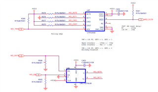
I'd need to know what is correct sequence for SET0, SET1 signals if I switch between WD disabled (SET0 = 1, SET1 = 0) and 9ms / 195ms setting (SET0 = 0, SET1 = 1). So it requires changing both signals. Can I switch both signals same time in this case? I attached a schematic for illustration. If I can switch only 1 signal at time then I'd have incorrect WD setting which I cannot easily change, so I don't know how to set SET0 = 0, SET1 = 1 in this case. CWD = 10k to VDD, so I don't use programmable CWD.

Thanks

Best regards

Libor

  • Hi Libor,

    The only way to switch the SET pins is doing it one at a time.

    There is a 500us delay between changing the state of the pin and reset needs to be asserted.

    Best,

    Andrew

  • Hi Andrew,

    if I switch only one pin then I enable WD with "SET0 = 0, SET1 = 0" or "SET0 = 1, SET1 = 1" mode, but I need "SET0 = 0, SET1 = 1". So it means I enable WD in different mode and then I need to switch to "SET0 = 0, SET1 = 1" but I'm not sure if I can simply switch mode when WD is running, I guess not but please let me know. Can you please describe the correct sequence for switching device from "SET0 = 1, SET1 = 0" (WD disabled) to "SET0 = 0, SET1 = 1"? Please let me know the sequence for both ways (disabled to enabled, enabled to disabled). Thanks a lot!

    Best regards

    Libor

  • Hi Libor,

    If I understand your situation correctly, then this exact use case is covered in the TPS3430 datasheet

    Please let me know if this answers your question or you need further explanation.

    Best,

    Andrew

  • Hi Andrew,

    let me ask other way. Datasheet shows 2 pictures with a sequence where both SET0 and SET1 are changed with the 500us delay (Figure 6-3 and 7-4). But the pictures show also a drop on VDD1, VDD2 which is described as reset event, but switching the device supply voltage below UVLO is complication for design (complex schematic for WD device), so probably I would not use this device for our application in this case. I'm not sure if these pictures 6-3 and 7-4 are applicable to my case because it seems to me strange that switching from "WD disabled" to modes "SET0 = 0, SET1 = 0" or "SET0 = 1, SET1 = 1" is very simple and switching to mode "SET0 = 0, SET1 = 1" is very complicated. So if switching between "WD disabled" and "SET0 = 0, SET1 = 1" mode is used then is it necessary to apply just 500us delay or is it necessary to apply 500us delay and the reset event by switching power supply below UVLO?

    Thanks!

    Best regards

    Libor

  • Hi Libor,

    Sorry for the misunderstanding on my end. I would suggest switching over to TPS3436CCCBGDDFRQ1 as it has an independent WD-EN pin as well as SETx pin for scaling. 

    This should solve your issue of switching from Setx=01 to Setx=10 without triggering a reset assertion

    Best,

    Andrew