This thread has been locked.

If you have a related question, please click the "Ask a related question" button in the top right corner. The newly created question will be automatically linked to this question.

Buck-boost or Discrete solution requirement

Other Parts Discussed in Thread: LM5118, LM5177

Hi,

I am looking for a device or strategy which can suffice below requirement:

  • Supply voltage: 12V/ 24V battery system 
  • Load dump voltage: 45V
  • Cold-crank voltage: 2.8V to 3V 
  • Regulated output voltage: 3.3V
  • Output current: 2A

Can LM5118 fulfil this? Is there another better solution or discrete design

Regards,

Prachi

  • Hello Prachi,

    Please have a look at LM5177.

    Best regards,
    Brigitte

  • Hi Brigitte,

    Thanks for the suggestion. However, I was unable to get the details regarding cold-crank condition in the datasheet.

    Is there any document available to confirm LM5177 behavior during cold-crank? 

    Regards,

    Prachi

  • Hello Prachi,

    Cold-crank is an condition of an application but not for an semiconductor device. So you typically will not find cold-crank details in a datasheet.

    Nevertheless the device needs to fulfill this cold crank condition. So if you check with this condition the operation range of the device.

    Best regards,

     Stefan

  • Hi Stefan,

    I checked the operating region of LM5118, and Vin can drop down until -0.3V, according to the datasheet. 

    Will it sustain a cold crank of 100ms at 2.8V? UVLO and EN conditions are met, and Vin is in the range of absolute maximums. 

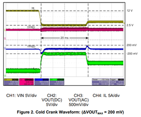
    I also referred to Application report SNVA741, figure 2 (attached below), showing similar condition for 20ms. Can it hold up to 100ms? How much current can it supply during this condition? 

  • Hi Amogh,

    please note: 0.3V is the abs max. rating of VIn.

    Operation is specified for VIN>= 3.0V.

    So the LM5118 can operate down to a VIN voltage level of 3V but also the power stage must be able to work with this voltage level:

    - Power and current rating of MOSFETs and Inductor and Sense Resistor needs to be designed for that.

    - If going down to that low voltage level the VCCX supply should be used to get the Gate drive signals high enough as this will be derived from VIN otherwise.

    Note: if VCCX is supplied (externally or from VOUT) this only should be connected to that signal once the power stage has fully powered up and the targeted VOUT voltage level has been reached.

    Best regards,

     Stefan