This thread has been locked.

If you have a related question, please click the "Ask a related question" button in the top right corner. The newly created question will be automatically linked to this question.

BQ76952: Charge FET damage at Regen in TIDA-010208 design

Part Number: BQ76952
Other Parts Discussed in Thread: TIDA-010208

We are using BQ76952 in a 16S BMS. In the event of an Over-current during charge, the AFE turns OFF the charge FETs by command of the microcontroller based on charging current thresholds. After the FETs were open, we observed an increase of voltage on the pack+ pin to 95V, followed by an unintentional rise in AFE CHG pin voltage driving the charge FET gate. This leads to charge FETs operating in linear regions and hence getting damaged.
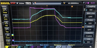
Signal definition:

  • Yellow: Charge FET gate w.r.t Ground(BAT-)
  • Light blue: BAT+
  • Purple: MATH function where it represents Charge FET gate to source voltage
  • Pink: Drain common to CHG and DSG FET w.r.t Ground(BAT-)
  • Dark Blue: Current where 1V represents 10A

Here is a snapshot where Charge FETs get damaged after shifting into a linear region

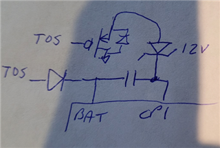
The Mosfet gate circuit followed in the above design is according to TIDA-010208.

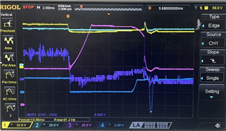
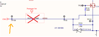
The following test was performed to deduce leakage in voltage from the AFE CHG pin by removing the current limiting resistor and measuring the voltage of the CHG pin.

Here, DSG FET and CHG FET were turned OFF, and the battery voltage was approximately 53V. On a surge of 135V on the PACK+, a voltage induced in the CHG pin and Charge pump was observed internal to AFE. This suspected rise in voltage could be the cause for charge FETs entering the linear region and, hence, the failure.

Signal definition:

  • Yellow: CHG pin w.r.t Ground(BAT-)
  • Pink: Drain common to CHG and DSG FET w.r.t Ground(BAT-)
  • Dark Blue: Current
  • Light Blue: CP1 pin w.r.t Ground(BAT-) ( hidden behind yellow signal)

  • Hello Embedded Developer,

    Yes, we have seen this happen before. This can happen when the LD pin is lower than the DSG pin, which causes an internal P-FET to turn-on causing the DSG voltage to reach the CP1 voltage. Normally LD being lower than DSG is okay as long as the voltage seen by DSG is below CP1.

    If the DSG voltage is greater than the CP1 voltage, it will cause CP1 to increase. This normally causes no problems, but if CP1 increases ~20-V above BAT, it will cause CP1 to start raising the BAT pin voltage, which causes the unintended turn-on of the CHG FET.

    There are a few things you could do to mitigate the problem:

    • Ensure LD does not go below DSG
      • This normally is not an issue if LD is connected to PACK+.
      • Since you are using the TIDA-010208, you probably have a Zener on LD, this Zener is likely why LD is going below DSG.
        • This however means LD may be exposed to very high voltages.
    • Ensure DSG does not see a voltage higher than CP1.
      • Voltage from PACK+ can leak to DSG if it is larger than the CP1 voltage. Sometimes adding back-to-back Zeners is enough if PACK+ is not going too much more above DSG, as seen below:
    • Clamp CP1 voltage to ensure it does not go above 20-V above BAT.
      • Zener + P-FET could work, something like seen below:

    Sorry for the troubles here. Let me know if you have any additional questions here.

    Best Regards,

    Luis Hernandez Salomon