This thread has been locked.

If you have a related question, please click the "Ask a related question" button in the top right corner. The newly created question will be automatically linked to this question.

UCC28064A: About OCP operation of UCC28064A

Part Number: UCC28064A

Hello!
I'm Takashi.
We are designing a power supply using UCC28064A.
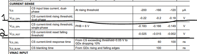
Please tell us about the OCP operation of UCC28064A.

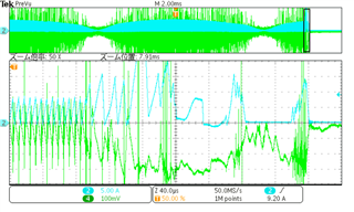
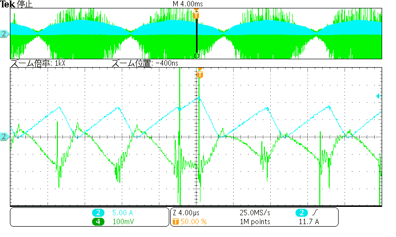
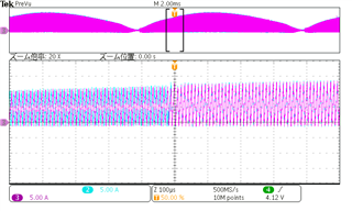
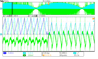
I will post the measured waveforms of the two-phase inductor current and CS terminal voltage when OCP operates.

ch1: Inductor current_B
ch2: Inductor current_A
ch4: CS terminal voltage

There are two things I want to know.
A) When OCP operates, the phases that were 180 degrees apart will overlap.
Is this behavior correct?
If this behavior is incorrect, please let me know how to fix it.

B) Current limiting by OCP starts in the middle of the sine wave.
Is this behavior correct?
If this behavior is incorrect, please let me know how to fix it.


Kind regards.

  • Hello,

    Your inquiry is under review and I will get back to you shortly.

    Regards,

  • Hello,

    Please see my comments below.

    A) When OCP operates, the phases that were 180 degrees apart will overlap.
    Is this behavior correct?  If this behavior is incorrect, please let me know how to fix it.

    >When OCP is triggered both phases will stop switching.

    >When OCP is cleared the two phase will come up in phase and then be phased shifted so they are 180 degrees of of phase.  This can take up to 10 switching cycles.

    B) Current limiting by OCP starts in the middle of the sine wave.
    Is this behavior correct?

    >I would double check this to ensure that the CS resistor is the correct value and if the design is an OCP condition.

    >If it is not a true OCP condition your CS resistor may too large.  This can be resolved reducing the size of the CS resistor.

    >If it is not true OCP and the CS resistor is the correct size, it could be noise causing the OCP fault.  This can be resolved by filtering on the CS pin.

    The following link will bring you to an excel design tool that you can use to check your component values.

    https://www.ti.com/tool/download/SLUC645

     
    Regards,

  • Hello!

    Thank you for answering.

    A)
    Do the two phases operate in the same phase even while OCP continues (while the CS pin voltage exceeds the threshold (-200mV))?
    The waveform I sent you is a continuous state of OCP.

    B)
    As you say, the CS resistance is currently larger than the designed value.
    I've also added a filter circuit to the CS pin.
    With the filter circuit, OCP is applied at the same level as the design value.
    If the filter is not effective, the IC will be damaged.
    filter constants
    1000pF+100Ω: OK
    470pF+100Ω: Damaged

    I was able to take a picture of the waveform at the moment of damage, so I will send it to you.
    This is an incorrect movement of the IC.
    Does this mean that the filter on the CS pin needs to be larger? Or are there other ways to prevent malfunctions?

    Light blue: inductor current
    Green: CS terminal voltage

    Kind regards.

  • P.S.
    The phenomenon in which the OCP starts operating in the middle of the sine wave can be improved by changing the capacitance of the ZCD pin from 22pF to 47pF.
    Is this solution approach okay?

  • Hello,

    Your inquiry is under review and I will get back to you shortly.

    Regards,

  • Hello,

    If the FETs are turning on CCM that is because noise has triggered the ZCD detection or the output has dropped below the input triggering a ZCD, even though one has not occurred.  

    You had mentioned that increasing the filter cap on the ZCD pins improves the behavior.  Most likely noise is triggering the ZCD and is O.K. to filter the ZCD pin. 

    Regards,

  • Hello!

    Thank you for your reply.

    I have an additional question.
    When the load is light, the phases of A and B do not shift by 180°.
    As the load increases, it will shift by 180°.
    Is this behavior correct?

    No measures have been taken to prevent malfunctions yet.
    It malfunctions at the same location on the sine waveform every time.
    I put a filter in the ZCD terminal.
    Are there any other measures?

    ch2: inductor current
    ch4: CS terminal voltage

    Kind regards.

  • Hello,

    The waveforms that you have attached looked to be 180 degree phase shifted.  The only issue that I see is you have one longer pulse.  It looks like the ZCD is false firing.  This is most likely due to noise and you may be able to solve this by filtering the ZCD pin/s.

    Regards,

  • Hello!

    Thank you for your answer.

    Question 1
    It was malfunctioning due to noise as you say.
    The malfunction was improved by suppressing the MOSFET Vds surge.
    This surge countermeasure has a large loss, so I would like to consider adding a filter to the ZCD terminal as a different countermeasure.
    So, up to what capacitance does the ZCD pin filter not affect control?

    Question 2
    There is a big difference between a load where OCP is applied and the A and B phases become the same phase, and a load where the output voltage begins to drop.
    The output voltage will not drop unless the load current is doubled after OCP operation starts.
    The design value seems to be the value at which OCP operation starts.
    Is this behavior correct?
    Is there a theoretical value that controls the point at which the output voltage drops?

    Best Regards.

  • Hello,

    Before diving into the questions.  You have mentioned that the FET surge was causing the issue.  Do you have bypass diode to handle the inrush current.

    If not this may resolve the issue.

    Regards,

  • Hello!

    A bypass diode is included in the circuit.
    Please answer the question.

    Question 1
    It was malfunctioning due to noise as you say.
    The malfunction was improved by suppressing the MOSFET Vds surge.
    This surge countermeasure has a large loss, so I would like to consider adding a filter to the ZCD terminal as a different countermeasure.
    So, up to what capacitance does the ZCD pin filter not affect control?

    Question 2
    There is a big difference between a load where OCP is applied and the A and B phases become the same phase, and a load where the output voltage begins to drop.
    The output voltage will not drop unless the load current is doubled after OCP operation starts.
    The design value seems to be the value at which OCP operation starts.
    Is this behavior correct?
    Is there a theoretical value that controls the point at which the output voltage drops?

  • Hello,

    Thanks for confirming the bypass diode was in place.  It it was not the surge current would go through the FET when it turned on and the UCC28064A would not be fast enough to recover.

    Question 1.

    There are resistors from the ZCD winding to the ZCD (RZcd) pin.  If you put a capacitor (Czcd) from ZCD to ground it will form a low pass filter.  The filter pole (fp) is controlled to these two components and can be adjusted.  I generally set the pole between 750 kHz to 1 MHz if it is needed.  Some customer will do it for less if there layout is not done well.  The UCC28064A data sheet gives an example layout and layout recommendations that can help you reduce noise in your system.  https://www.ti.com/lit/gpn/ucc28064a


    fp = 1/(2*3.14*Rzcd*Czcd)

    Question 2
    You had mentioned this occurs during inrush.  The FETs should stay off until Inrush is complete.

    One condition that can occur as mentioned previously the ZCD pins can false fire if the input voltage is  higher than the boost voltage.  This actually can happen during inrush.  The input voltage will be one diode drop above the boost capacitor.  If you are switching during this period it is possible to get ZCD misfires.

    The CS feature that turns the FETs off should only be used during inrush.  It should not be being triggered during normal operation.  Is your CS resistor the correct size?  It should be sized to handle 2X the inductor output current with 20 to 25% margin.  You might want to check that resistor value.  Please note that noise can cause this to false fire as well.

    Regards,

  • Hello!

    Your advice helped me. thank you.

    The remaining issue is operation during overcurrent.
    This is the content of the previous question ②.
    This phenomenon is not occurring at the time of rush.
    This phenomenon occurs when the load increases during normal operation and the overcurrent protection is activated.
    Overcurrent protection is applied and the peak current is not limited even if the inductor currents are in the same phase. Therefore, overcurrent protection is activated and a large current flows until the output voltage drops.
    I'll attach the waveform.
    Ch2: A phase inductor current (light blue)
    Ch3: B phase inductor current (purple)

    Is this behavior normal?
    I would like to design the inductor's peak current to reach a ceiling as soon as overcurrent protection is activated, and the output voltage to drop as the load increases.
    Is there any solution?

    Kind regards.

  • Hello,

    Your inquiry is under review and I will get back to you shortly.

    Regards,

  • Hello,

    If this is the case your current sense resistor may not be sized correctly.  You can check the value with the excel design tool that can be found at the following link.  https://www.ti.com/tool/download/SLUC645

    The other issue could be noise on the CS pin.  You could try adding filter capacitance to the CS pin to attenuate any noise that might be falsely triggering the OC detection.

    Regards,

  • Hello!

    Please tell me about OCP operation.

    The PFC setting constants match the constants in the design sheet we received from you.

    As the load is increased, the lowest oscillation frequency is detected before OCP operates, and the output voltage decreases.
    We check OCP by checking whether the inductor currents are in the same phase.

    First, is this behavior normal?
    Next, please tell me what to do if this behavior is not normal.

    Kind regards.

  • Hello,

    I am reviewing your inquiry and will get back to you shortrly.

    Regards,

  • Hello,

    When the current sense trips OCP (1, CS = -0.2V) both phases will turn off the FETs and will not turn back on until the CS pin goes above -0.015 (2).

    When the converter starts again after OVP is tripped both outputs will come up in phase.  So this is what you are observing and it is normal.

    Regards,

    Mike

  • Hello!

    Thank you for your reply.
    My question was bad, so I didn't get the intent of the question across.

    Question
    When the load is increased, the lowest oscillation frequency is reached before the overcurrent protection is applied, and the output decreases. Is this behavior correct?

    In my image, overcurrent protection operates first.

  • Hello,

    If the output is loaded and you trigger OCP the FETs will stop switching and the boost capacitor voltage will decrease.  That is what is expected.

    This function is really for inrush current limiting to protect the FETs.  PFC boost design are protected by the fuse and the down stream converters over current protection.  You might consider using the down stream converter to limit the power instead of the PFC front end.

    Regards,