This thread has been locked.

If you have a related question, please click the "Ask a related question" button in the top right corner. The newly created question will be automatically linked to this question.

UCC14240-Q1: Top Vgs stability under Bot switching issue

Part Number: UCC14240-Q1
Other Parts Discussed in Thread: UCC21750,

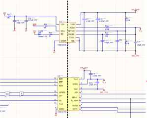
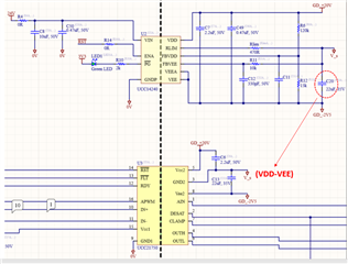
Hi, I am having some trouble with our UCC14240-Q1 implementation, we are using the UCC14240-Q1 in combination with the UCC21750 gate driver for a VSI design. In the picture below DPT data can be seen.

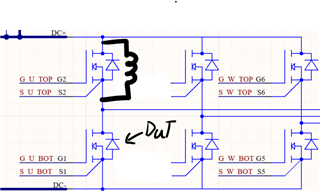
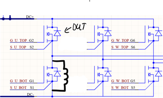
The pictures on the left shows bot as the DUT, while the Vgs measurement is of the top MOSFET. The picture to the right is when the top MOSFET is the DUT and the Vgs measurement is of the bot MOSFET.

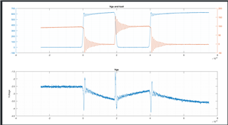
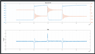
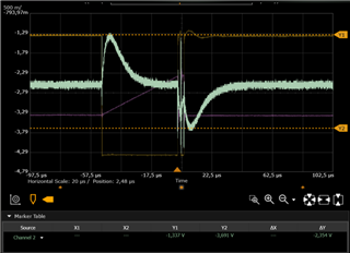
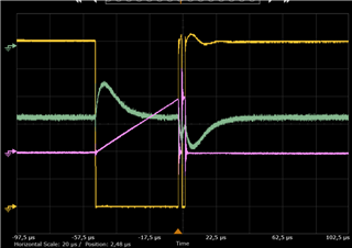
The issue seems to arise whenever the DUT switches, and has a very slow response time. As a similar drop of Vgs also happens at the start of the first long pulse when the DUT turns on the first time. picture of this can be seen below. (first spike is up to -1V3 from -2V5 and second spike is down to around -3V6)

Any input into what could be causing this would be greatly appreciated.

  • Hi William,

    I am taking care of this thread and I will be back to you later today.

    Thank you

  • Hi William,

    Would you please provide schematic of both the system (as you mentioned top and bottom I assume you are talking about a half bridge or a full bridge?) and the schematic around UCC14240-Q1 and UCC21750 (components around the device). I also have some questions about your comments:

    "The pictures on the left shows both as the DUT": Do you mean (UCC14240-Q1 and UCC21750) right? Are these connected on the bottom or left switch? Could you point it out in your schematic?

    "The issue seems to arise whenever the DUT switches": Do you mean the top of bottom switch? Could you point it out in your schematic? Would you please label your waveforms in yellow, green and pink, and show the V/div?

    The schematic around UCC14240-Q1 is particularly important to see if component placement is correct. How did you design your component selection? Did you use the Design Calculator pointed out below? Please, also provide switching frequency fsw and gate driver voltages.

    Thank you.

    UCC14240-Q1 Design Calculator

  • Hi, thank you for answering, I must apologize for a unclear message. Yes I was referring to a half bridge when writing Top and Bot. I also see that my use of DUT was a bit confusing. When referring to DUT I am referring to the MOSFET in the double pulse test. I have also added a picture of the UCC14240-Q1 and  schematic:


    For your first question, The left picture is of DPT data when switching the bottom switch while measuring the gate voltage of the top switch. 

    While the right picture, is the opposite, where the Top switch is the DUT and is the one switching, while measuring the bottom MOSFET gate voltages. as shown below.

    The last picture depicts the entire double pulse test pulse both the long and short pulse.  The Yellow trace is the Vds of the bot mosfet and has a 100v/div while the pink trace is current measured at source of the bot switch and is 50A/div. while the Green is the Vgs of the Top switch. I have added a better picture of that bellow:

    When designing, we did use the design calculator, at that time we used the V6 version.

    The switching frequency designed for is 20k Hz and gate driver voltages of +20V / -2V5 

  • Hi William.

    I will be back to you tomorrow morning. Thank you

  • Hi William

    I can notice from the last picture (black background) that the bottom switch is having some problems when turning OFF. You can notice that is turning OFF, then turning ON and finally turning OFF with a very high frequency. First, could you please check (probing) the driver PWM signal applied to (VCC-GND)? One option is that the driving signal might be disturbed for some reason.

    Also, I reviewed your schematic and I have one observation. Everything looks good but the placement of C20. C20 is a 22uF cap that is connected at (COM-VEE) at the bias supply side. This extra 22uF cap (you already have C13 22uF cap between (COM-VEE) at the gate driver side) might affect the voltage balance at the COM pin, increasing the pull-out current needed through RLIM, and consequently decreasing the max value of RLIM and decreasing the efficiency. Please connect C20 at (VDD-VEE) at the gate driver cap. This cap at the gate driver side will improve the balance voltage at COM pin and then decreasing the pull our current needed through RLIM, and consequently increasing the max value of RLIM and increasing efficiency. Just change the position of C20 and check if there are any improvements.

    PS: In your DPT waveforms I noticed that the orange waveforms is labeled as Icoil, however it does not look like the inductor current but as a Vgs pulse. Inductor current should look triangular as it is increasing during the ON time of the main switch. Also, would you please confirm that VCC2 (schematic) is equivalent to VDD (Datasheet, Pin Configurations) and VEE2 is equivalent to VEE (Datasheet, Pin Configurations)?

    Thank you

  • Please, find attached Design Calculator V.8 that I did for your UCC14240-Q1 Schematic. I assumed a 30nC gate charge for your switch. The difference between V.6 and V.8 is that V.8 introduces the Cout1B capacitor connected between (VDD-VEE) at the gate driver side. This capacitor, as mentioned above, improves the balanced voltage at COM, Increasing the RLIM max value and improves efficiency.

    UCC1424x-Q1_Calculator_V8_RevolveNTNU.xlsx

    Thank you