This thread has been locked.

If you have a related question, please click the "Ask a related question" button in the top right corner. The newly created question will be automatically linked to this question.

LM3150: Doubts about positioning, routing and signals for buck converters

Part Number: LM3150
Other Parts Discussed in Thread: INA226, LM22673, LM22679, CSD18537NQ5A, CSD18504Q5A, LM5117, LM5166, LM25018

Good morning,

I have been using the Buck converter LM3150 for some time for many of my projects, where however the spaces are usually larger.

This time, however, the size of the card forces me to use a more "restrictive" layout.

I followed the Webench project which suggested the following to me (if you need the P/Ns suggested by Webench I'll pass them on to you)

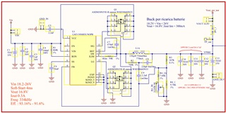
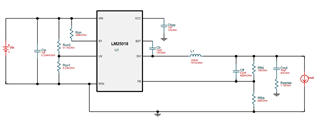
/resized-image/__size/1739x889/__key/communityserver-discussions-components-files/196/2_5F00_1schematic.jpg

Unlike the original Webench scheme I only divided the feedback resistor Rfb1 with 2 resistors, one fixed and one with a potentiometer which, being of necessity
SMD size (Burns 3224W series) is only 12 turns and therefore to obtain a conversion value the as close as possible to the desired I need to decrease the resistive
value of the trimmer by putting a resistor in series.

The buck converter values ​​will be as follows:

Vin : 13.2 - 28V
Vout: 12.06V
Imax : 10A
Soft start: 4ms
Frequency: ~ 474kHz


I attach you below:
- The Outline

/resized-image/__size/707x1064/__key/communityserver-discussions-components-files/196/3_5F00_outline.jpg

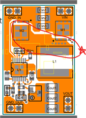
- The Top Layer (the orange is the copper of the TOP, I also marked the paste in gray (because I couldn't show the PADs well) and in black the outline with
the component references).)

/resized-image/__size/3297x4945/__key/communityserver-discussions-components-files/196/4_5F00_top.jpg


- Inner Layer 1 (the orange is the copper of the internal side 1, I also marked the VIAS in gray and the outline in black with the refs of the components present
at the TOP in those areas)

/resized-image/__size/707x1064/__key/communityserver-discussions-components-files/196/5_5F00_inner1.jpg

- Inner Layer 2 (the orange is the copper of the internal side 2 which is entirely GND lake, I also marked the VIAS in gray and the outline in black with the references
of the components present at the TOP respectively in those areas)

/resized-image/__size/707x1064/__key/communityserver-discussions-components-files/196/6_5F00_inne2.jpg

- The Bottom Layer (the orange is the copper of the internal side 2 which is entirely GND lake, I also marked the VIAS in gray and the outline in black with the
references of the components present at the TOP respectively in those areas)

/resized-image/__size/707x1064/__key/communityserver-discussions-components-files/196/7_5F00_bottom.jpg

To carry the 10A I preferred to make it in 4 layers of which:
- inner 2 (18um copper) and the Bottom (35um copper) entirely dedicated to GND
- Top (35um copper) and Inner 1 (18um copper) dedicated to the positive and signal tracks.
I have often read to put at least 1 full side of GND so I also passed the signals on the MOSFET gates to Inner 1 or to the TOP.

I added some Vias on the inductance pads to increase its dissipation on the internal layer and the same thing under the thermal pads of the 2 mosfets in order

to increase the copper on the internal side.

Now the questions:


1) do you think the layout is fine and does not create problems? (I tried to put all the capacitors and resistors as close to the controller as possible)
2) I could also make the PCB 6 or 8 layers by simply duplicating the inner 1 and the inner2 each 2 more times towards the inside so as to have 4 sides for the

positive signal and 4 sides for the GND. Could it help or could it cause problems?

3) among the options given by Webench it initially suggested the 4.7uH inductance that he suggests for the 6.8uH XAL1010-682MEB inductance, do you think it's good?

Because I wouldn't want the inductance to heat up unnecessarily if the load was much lower than that for which I assumed its use (since the use was designed for

multi-purpose purposes, i.e. both for "low" load applications 2-3A,both for applications with 8-9A load)

4) I had a doubt, does the LM3150 have DCM (Discontinuous Conduction Mode) ? Because I didn't find it on the datasheet by doing a search.

5) do you have any suggestions for the future of some tracks or signals that absolutely must not pass through certain areas?

Thanks everyone in advance


Paolo

  • Hello Paolo 

    1. Since the noise across the low-side feedback resistor directly affects the operation of the COT device, if possible please use the potentiometer in series with the high-side feedback resistor. Also, you can minimize a noise-coupling if you insert the  ground layer between the top and the inner layer1. Please don't forgot connecting the ground connection of the low-side feedback resistor directly to the #5 SGND pin. 

    2. It helps always.

    3. Lower inductance is better if you'd like to reduce the solution size / increase the efficiency. Lower inductance also helps increasing the VOUT ripple to make COT device operation stable. 

    4. https://e2e.ti.com/support/power-management-group/power-management---internal/f/power-management---internal-forum/404258/lm3150-excessive-inductor-current-at-no-load?tisearch=e2e-sitesearch&keymatch=LM3150%2525252520DCM# 

    5. I wish you can reduce the switching node area. The smaller switching area helps reducing the ringing at the SW node and also helps reducing the EMI. 

    -EL 

  • Hi Eric, thanks for the reply. Below I will reply with the changes made.

    1) I moved the potentiometer in series with Rfb2 (I still have to change the values, now I'm focused on the layout) and I connected the pin that goes to ground of Rfb1 directly on pin 5 of the integrated circuit, was this what you meant?


    2) I brought the number of total sides to 8 to increase dissipation. Alternating 1 positive signal/power supply side with one GND side, is this correct? Because from how you wrote in point 1 you made me insert the GND Layer between the TOP and the internal doubled Layer of the power. Following this I continued by placing 1 positive and 1 negative. It could go well? (the TOP and BOTTOM always 35um while the internal ones are all 18um)


    3) As regards the inductance, I would say that the efficiency between the 4.7uH and the 6.8uH changes very little (from 96.4% to 95.7%) while the size would be the same since the package is the same

    For the inductance there are 2 choices: the 4.7uH XAL1010-472MEB or the 6.8uH XAL1010-682MEB

    My Buck will basically work at 1.5A - 2A. I oversize it because the loads I connect to it in the future could require up to 10A.

    The Lipp values ​​that come out of Webench with the 2 inductances are the following: the 4.7uH one has Lipp of 3.07A (and its half is equal to 1.53A), while the 6.8uH one has Lipp of 2.13A (whose half is 1.06A). In the second case it would be more difficult to enter DCM.

    The low inductance on the one hand therefore helps the COT stability, but in the case of low loads it would enter DCM more often

    The higher inductance would help COT stability less, but with low loads it would be more difficult to go into DCM.

    What do you recommend in my case?

    4) the attached link won't open for me. What was discussed in that link regarding DCM?

    5) I reduced the distance of the switching node like this, do you think it's ok?

    I reposted all the positioning and layers for you.

    Thank you very much for helping

  • Hello Paolo 

    1) Yes, correct.
    2) Yes, correct.
    Please connect the VIAs underneath the LM3150 DAP to the grounds in the inner layers.
    Please connect GND_IN and GND_OUT to the grounds in the innner layers.
    3) It seems 4.7uH is better.
    4)

    5) It is better now. 

    -EL

  • HI. You're right, I noticed that the Vias and the connectors were strangely not connected on the internal sides 3 and 5... how strange, but thank goodness you also noticed because the electrical check had already passed! Just to be sure you meant to connect the GND on the internal sides 3 and 5 which you didn't connect right?

    Another thing... can I leave pin 3, the EN disconnected if I don't use it right?

  • Hello Paolo 

    Yes, I meant inner layer 3 and inner layer 5. 

    -EL

  • Ok.thanks! Another thing... can I leave pin 3, the EN disconnected if I don't use it right?

  • Hello Paolo 

    Yes, you can leave it floating. 

    -EL

  • I ask you one more thing, maybe you have already used it.
    Could 3 classic 2.54mm pitch headers be enough to carry all the current (10A)? (3 on VIN, 3 on GND, 3 on Vout and 3 on GND out)
    Because I read that the pin strips carry a maximum of 3A. By putting 3 of them I would be at 9A max....I looked on the manufacturers' websites and there are male pin strips that carry a maximum of 5A (only because they are gold plated, because the size of the pin is always a square with a side of 0.64mm) , but their printed female would still carry 3A.. Do you think I'm binding my head too much or would it be appropriate to put another type of connectors? Do you have any suggestions?
    I also thought about putting 1.27mm pitch pin strips which would each carry 1A
    In 5.08mm I would put 3 2.54mm pins for a total of 9A and instead I would be able to put 10 (2 rows of 5) of 1.27 headers which would bring 10 x 1A = 10A.

    Other suggestion in 5.08mm max space?

    What do you think?

  • Hello Paolo 

    You have to consider not only the current rating of each metal pin, but also the contact resistance which you can control in your manufacturing line. Based on my experiance it is very hard to control the contact resistance of the pin which you are trying to use, if the contact resistance is too much then your connector can be burnt out. (For example, 10A^2 x 100m ohm = 10Watt). I use screw type connector if the load current is large. 

    -EL

  • Eh...you're right because the pin might not hold.
    I found this 2.54mm pitch male header from SAMTEC (TSW-103-14-G-S) that promises to handle 6.3A when paired with its female header (SSQ-103-01-L-S).
    On their website on the TSW product page coupled with the SSQ there are test reports on the power carried out on the pin.
    From what I see it can deliver 4A to the pin with a calculated resistance of 3.85mOhms.
    With 2 pins it seems to have reached 8.61A with a connector temperature of 35°C.


    if that were the case and I put 3 of them in there I would say that I would have to stay largely inside since I would have the maximum 10A brought to 3 and therefore the values, even if they were the absolute worst, I would have the pin at 35°C. Am I right?

  • Hello Paolo

    You have to contact SAMTEC to get the answer. 

    Again, the contact resistance is not guaranteed by the connecter manufacturer.

    -EL 

  • Ok perfect thank you very much. I will try to contact SAMTEC for answers on this.
    In the meantime, I'm also asking you about another PCB that I had set up some time ago. I will probably have to retouch the layout following a similar placement to that of the betting slip we were talking about before, but apart from this, how do you see the scheme and its use?


    I'll explain: since I already knew the integrated circuit I had opted to use the LM3150 to recharge lithium batteries.
    I know that there are chips specifically to act as a charger, regulator and BMS for the batteries but my request is different and I cannot use a chip already made and I will explain why.

    I'm building an almost "in-line" UPS, meaning that in the absence of line voltage the load immediately takes power from the batteries without having any "gaps".
    The lithium batteries (in my case 4S) would be constantly and always under charge and in order not to deteriorate their life I thought of keeping their maximum charge at 16.8V (4.2V x 4), of creating a circuit for balancing them and overcharge protection.
    Therefore I thought of using the LM3150 chip to regulate the output voltage from 24V to 16.8V that goes to the BMS which protects the batteries, and also through the Rlim limit the charging current of the batteries to 300mA, so that the first charge is slow and then that the power "lost" in the balancing circuit is quite low (300mA allows me to recharge the batteries to 100% for the first time in many hours, but slow charging is good for them, furthermore once they are all charged to avoid the excessive charging the current will pass into the 47ohm 1W R and will be dissipated.
    Obviously there will be a microcontroller with which I will read the current (which since the batteries are in 4S series will be the same for all), the temperature and the 4 voltages of the individual batteries so that if I notice problems or anomalies the microcontroller will drive a mosfet which will immediately disconnect the entire circuit, sending it into protection.

    Now my question is is it okay to use the LM3150 for this purpose? In the end, with the LM3150 I would impose a maximum voltage of 16.8V (and once it reaches that level the batteries will stop recharging) and a current limit of 300mA.
    During the balancing the 300mA will be "lost" on the 47ohm resistors, while once the balance is reached the current supplied will be practically zero and the DC-DC will continue to convert the 16.8V to keep the batteries charged which will be protected by the BMS designed to hoc through
    - INA226 ADC (for current and voltage readings)
    - DB18S20 temperature sensors
    - HY2213-BB3A balancing module

    What do you think?

  • Hello Paolo

    Please refer my comments below 

    LM3150 current limit has a wide variation. If the BMS regulates the battery charging current , it is okay to use. If not, you need to use an external circuit together with a peak current mode controller to regulate buck converter output current. 

    Also, I think you don't need to use a controller since the load current is only 300mA. You can use a converter device with integrated FET. 

    -EL 

  • Um...then my goal would be for the Buck to generate a fixed voltage for me and also limit the current.
    What do you mean "has wide variation"? Do you have a precise value of how much this variation could be or if set for example at 300mA could it also become double or more? Because if you tell me that it could be 300mA or 280mA or 320mA it doesn't change anything for me (because 300mA is a value that I chose so that my batteries are recharged very slowly) but if from 300mA the current became 600mA or even 1000mA, well there would be a difference and all the calculations on the battery balancing circuit would go wrong.
    What would you suggest?

    On the LM3150 I can't find the current accuracy.
    More than anything else, I don't understand whether this current value would fluctuate continuously (so one second before it is 400mA and one second after it could be 300mA) or whether the limitation value could vary from the calculated one but would always remain fixed (therefore always at 400mA or always at 225mA for example due to the manufacturing precision of the integrated circuit itself)

    "Also, I think you don't need to use a controller since the load current is only 300mA. You can use a converter device with integrated FET. "
    In fact the LM3150 could fit, it's almost exaggerated in fact for only 300mA, the problem is that I haven't found an easy to solder controller (without strange or complex packages to solder) that has a current limit. Do you know any?

    In the meantime I looked a bit and in case I confirmed that the current values ​​in the LM3150 vary a lot, I saw that there are converters with integrated FETs such as the LM22673 or LM22679 the problem is that in both the minimum current limit that can be set is however higher 300mA in the figure in the datasheet. I really can't find the formula for calculating the R ilim in their datasheets...

  • Hello Paolo 

    The current limit sensing pin source current has +/-12% tolerance. It is in the EC table

    RLIM tolerance can be +/-1% or +/-5% depending on your component selection. 

    RDS(ON) variation also depends on your component selection. There is ~50% variation from 25degC to ~ 130decC if ASDM30N55E.

    Please see the section 8.3.4 in the datasheet for more information. 

    -EL 

  • Hi, I looked at point 8.3.4 but it's still difficult for me to calculate the resistance.
    That is, the first 2 formulas are these

    Iocl = It is the value I would like, i.e. 0.3A

    delta IL = the peak peak of the inductor current ripple i.e. in my case 120.15 mA

    So Icl = 0,2399 A

    Why Icl (that is the current limit) is minor than the my choice 0.3A?

    Then RDS(on)max for the Low Side FET CSD18537NQ5A is 17mΩ and the I lim-th is 85 uA

    So Rlim = 47.98 Ω  while the Webench sugest me to use a 59Ω  for Rlim... the calculate are correct?

    If I do the calculation in reverse knowing Rlim, RDS(on)max and I lim-th the Icl comes out to 295mA

    I don't find where to find "The current limit sensing pin source current has +/-12% tolerance. It is in the EC table"

    How ever u tell me that my current limit so would be between 264mA and 336mA ?

    And will the current continually fluctuate?

    Will the tension remain fixed?
    Speaking of lithium batteries, the voltage must never exceed the maximum value of 16.8V total

  • Hello Paolo 

    is minor than the my choice 0.3A? ==> Average current is less than peak current. 

    the calculate are correct? ==> Correct

    I don't find where to find "The current limit sensing pin source current has +/-12% tolerance. It is in the EC table"

    ==>

    would be between 264mA and 336mA ? ==> I think you haven't considerred the RDSon variation

    -EL

  • would be between 264mA and 336mA ? ==> I think you haven't considerred the RDSon variation

    So you mean that the calculation of +/- 12% should be done on the Icl that I would have calculated?
    That is, +/- 12% should be calculated with respect to 0.2399 A?

  • Hello Paolo

    For example, if the Rdson variation is ~ 50%, your current limit variation should be at least 50%. 

    -EL 

  • Hi Eric, but I'm not clear, there are one low side and one high side mosfets. In the diagram I proposed to you, there are 2 identical ASDM30N55Es in both LowSide and HighSide. If I were to replace them with those suggested by Webench (which could be the CSD18504Q5A in the High Side and the CSD18533QSA in the Low Side), would things change?
    Since they are different, will I therefore have 2 different currents in the 2 states?
    In this case how will I see what current limit I will have?
    However, from the point of view of the variation of the Rdson I don't think it changes much since these also have between 25°C and 125°C at Vgs of 4.5V a variation from 1 to 1.5 of Rdson therefore also in this case a +50% of the value

    But sorry, I don't understand how Rdson can be variable? The temperature once you fix a load is... that is, on mosfets that carry 40A, letting 0.3A pass will bring the T junction to a few degrees above the ambient one. maybe 35-40°C so the value of its variation will be truly minimal and will be of the order of magnitude from 1 to 1.05-1.08 and therefore compared to 1.50 it would have a variation of only 10-15%, am I wrong?

  • Hello Paolo

    MOSFET RDSON variation will be changed by using CSDxxxx MOSFET, but the difference will be not so much big.

    Blue line is the RDSON variation when the gate voltage is 4.5V. Red line is the RDSON variation when the gate voltage is 10V.
    If you need more accurate data, you have to ask the MOSFET manufacturer to provide the RDSON variation data at 6V.

    If you are okay with the ~50% current limit variation, I don't have any concern. Please double check your system requirement. 

    You have to find the minimum RDSON at the lowest ambient temperature at no load, and find the maximum RDSON at the highest junction temperature at full load.

    -EL

  • Hi Eric,

    So let's think, the batteries are lithium batteries with a maximum charge of 4.2V and a nominal capacity of approximately 3400mAh (after a test the 4 batteries have a maximum capacity between 3200mAh and 3350mAh).
    Lithium batteries are usually recharged with a current 1/10 of their capacity so in my case 320-335mA.


    Now if the variation was 50% and I imposed an I lim at 300mA, 150mA < I lim < 450mA is perhaps a little too high.


    If I imposed I lim= 200mA I would have 100mA< I lim <300mA.


    Of course, if it charged at 100mA it would mean that to fully recharge them being in series they would take around 33 hours since they are 3300mAh, which compared to the 11 hours that I initially expected in the event of a second short blackout I would risk not having them charged enough. I have to think carefully...

    As for the output voltage, is that very precise? Because I have the balance that intervenes so that each does not exceed 4.2V, but I would like to understand if once I have found the value with the potentiometer on the output and set it to 16.8V this value remains stable for me or not. How much would the Vout tolerance be?

    Because in the meantime I'm looking at some chips for charging lithium batteries, but


    1) not all of them allow you to have the negative of the last battery directly connected to GND (and this would therefore prevent me from having a common GND with the ADC and the microcontroller to carry out the measurements and controls)


    2) almost all battery charger chips stop powering them once they reach 16.8V (this means that by no longer powering them until they drop to 4.1 or 4.0V it happens that every time several days pass and the battery voltage drops the chip starts a new charging cycle again to bring them back to 4.2V and so on... and in the long run this inexorably leads to a sudden deterioration of them following the increase in their charging cycles)


    3) require a much greater number of accompanying components.

    Do you know anyone else who might not be like this?
    Otherwise I have to find the solution with the LM3150

  • Hello Paolo,

    If you need more accurate current regulation, have you considered the LM5117, it has a current monitor pin and its more accurate.  you can also follow the guidance in the application note pertaining to CC/CV.

    Hope this helps.

    ti.com/lit/an/snva829/snva829.pdf?ts=1708619128259&ref_url=https%253A%252F%252Fwww.ti.com%252Fproduct%252FLM5117

    David.

  • Hi David, I looked at the LM5117, it's nice but it's very complex.. and above all it needs a lot of passive components and the space available isn't a lot considering that you also have to follow a layout for optimal operation.
    Since the charging current is very low I was also thinking of something that had the MOS already integrated (0.3A shouldn't be a big problem and also for the calculation of the Rdson etc. having it internally the values ​​in the tables already give the definitive values) .
    I looked and found some, but I need your more technical opinion on whether I'm wrong or not:


    - LM22673 seems to have an adjustable current limit but it seems that its variation could be +35% / -25% and from the graph it doesn't show me a value lower than around 1.8A (it doesn't show it because it couldn't get there?) The voltage instead, what tolerance would it have?

    - LM5166, it would be excellent because it requires very few components, it is synchronous, and has a limited current, only it is not clear to me what the "Programmable Peak Current Limit Supports" is: – 500-mA, 300-mA, or 200-mA Loads".   Is it possible to set an output current limited to 300mA? What would be its tolerance on maximum current? How much is the tolerance on the max output voltage?

  • OK Paolo, if you need a crude CC regulation, you can use a device in current limit, the device must have peak and value limit.  the average current at the peak and valley will be your regulated current.  If you are charging a super cap for example, these schemes work perfectly.  of if you need a CC operation as a max IOUT limit mechanism.

    Unfortunately, the LM5166 is not programable.

    You should look for a constant on time control, with Peak current limit and a peak current limit off timer, or a device that has peak and valley control using current mode control.  

    for example, the LM25018, is a 300mA device, perhaps that will work?

    Hope this helps.

    David,

  • Hi, David,
    in fact the LM25018 would be perfect both for component space and for the current limit.
    Only thing: in your opinion, using a buck that has a maximum current of 300mA always powered (because this will go into the UPS project so the batteries will always be powered and therefore the output will always be 300mA) will be fine or the chip after a while Will he start to suffer over time? For example, MOSFETs or other devices are usually taken at a rate of 3-5 times the maximum current that can pass through them to prevent them from overheating too much.
    Could this LM25018 be good for delivering 24/24 and 7/7 300mA?

  • Hello Paolo,

    As the battery voltage increases, the control scheme will automatically shift from CC to CV regulation.  So, it will no longer be supplying the full 325mA of current.  PS, even if it did, this device is rated to deliver 325mA of output current.  set the feedback resistors to the voltage you want to keep the batteries at during "float" region.

    NOTE: This device as a pseudo valley limit, it's a peak current limit off timer.  that's to say if the peak current limit level is violated, an off timer will engage and hold the LF FET on and the HS FET off, bringing the inductor current to a valley limit level, the off timer is dependent on the FB voltage.  if the batteries are fully discharged, the feedback voltage will be low, and the off timer will be long.  as the battery begins to charge the feedback voltage increases and the off time will decrease. additional note, the average current to your batteries will be the average current between the peak and the valley limit.  please refer to the table for the min max specifications of the peak limit and the off timer which will ultimately determine the average current to your batteries.  note that the specification is loose so over temp the limits will shift and the average current will be moving.  Your inductor value will also be a significant factor for determining your valley limit.  a larger inductor will deliver more average current because the valley current will be higher for a given off time (less ripple).

    I hope this makes sense. 

    See below a sketch to help you understand what I am describing above.

    As you can see, this is a crude implementation, but it is simple, you do have some control on where the average current will sit by carefully calculating the variation and selecting an appropriate inductor.  if you need something accurate, you will need a specific scheme which will require a lot more circuitry.

    hope this helps.

    David.

  • Hi David, I looked at the LM25018 and yes, it might be fine; I tried to follow the datasheet, but some calculations don't add up compared to when they are generated by Webench. As soon as I can I'll bring them back to you so we can analyze them together.
    Thank you

  • No Problem Paolo,

    Thanks.

    David.

  • HI. Forgive me but I was urgent about another project and I put this one aside for a moment.
    I then created an Excel file with the calculations relating to the LM25018 which I carried out based on what was reported in the datasheet.

    LM25018.xlsx

    If you have a chance, check it for a moment because there are a few things that don't add up to me.
    I am attaching the electrical diagram that Webench generates for me, which is partly correct and partly seems to me to generate values ​​that are not very correct.

    the only difference compared to the webench scheme is the insertion of a potentiometer (after Rfbt1 which will not be 10k but 8.7K) so as to be able to more precisely adjust the output voltage to the value I want of 16.80V

    My values ​​are as follows:

    VALUES PROJECT
    Vin min 20 V
    Vin nominal 24 V
    Vin max 28 V
    I out 0,3 A
    V out 16,803 V

    1) From the datasheet the fSW should have the following formula:

    and therefore from the calculations it should come out at around 604 kHz with a Ron of 309kΩ, however on Webench the fSW comes out at 544 kHz (which is very similar to the fSW(max) calculated with Dmin/Ton(min) )

    2) Then on WeBench he inserts an inductance of 150uH, but WeBench calculates everything based on the fSW of 543 kHz, while I get L1 of 130uH but with an fSW of 604 kHz

    3) The input capacitor calculated according to the formula:

    choosing an input ΔV of 0.5V (imagining that I can vary for example between 23.5V and 24.5V) the Cin comes out at 24.82uF while Webench suggests the 1uF one which is lower, why?

    4) Finally I have a question precisely about the peak current: the peak current calculated according to the formula :

    I find it to be 337mA which is < 390mA (which from the datasheet is the minimum current limit threshold)
    So what happens if the calculated peak current is smaller than the minimum current limit threshold?

    At the moment these doubts have arisen about it, I hope I'm not too wrong in order to avoid mistakes. I have already placed the PCB a bit and it seems excellent also in terms of size and space occupied.
    If we can resolve these doubts, I will show you the placement, whether it is correct and whether it can create problems, asking you for suggestions on the matter.
    Thank you
    Paolo

  • Hi Paolo 

    Is it possible to create new post if you have a question about LM25018 device?

    -EL

  • Hi Eric,
    you're right, I thought about it the other day too, but I already said that we started talking about it here, I thought I'd continue.
    To avoid problems I created a separate post of which I provide you with the link

    https://e2e.ti.com/support/power-management-group/power-management/f/power-management-forum/1332990/lm25018-doubts-about-the-desired-values-and-placement

    The only thing I ask you, however, is to keep this post active because when the PCB and components for the LM3150 board arrive, if there are any problems I will link directly to this post to talk about it, ok?

  • Hello Paolo

    I wish you can create a new post when the board arrives, but you can keep this post active if you want.  

    -EL