This thread has been locked.

If you have a related question, please click the "Ask a related question" button in the top right corner. The newly created question will be automatically linked to this question.

UCC3895: UCC3895 full bridge emission issue and switch on/off ringing

Part Number: UCC3895
Other Parts Discussed in Thread: UCC37324

Hi.


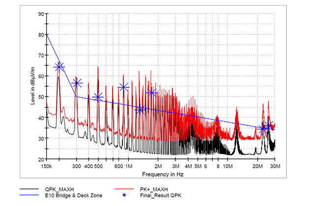
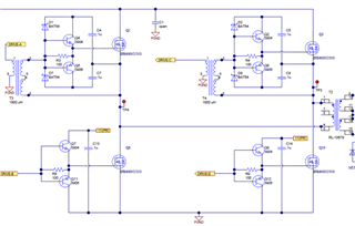
We are currently investigating one of our customers amplifier design that has UCC3895 full bridge driver making the +-180voltages for the AMP. The issue currently is that it is failing the radiated emissions in the 100kHz-30MHz area, mainly in the 100kHz-1MHz region. Issue could be sligthly improved with input side filtering and case emc shielding, but these modifications were not enough.a

Now that we have been studying this more it looks like it could be the UCC3895 driven FET's and their ringing that could be causing it. There could be also some other things to tune since the high side FET turn on and off has glitches every now and then.

For some reason the design doesn't follow the TI reference design and we have no notes or testing results why this design was used.

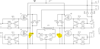
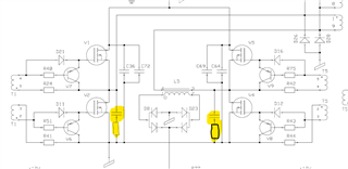
As we can see there is some improvements to be made at least on the switch on side and the switch on ringing can also be seen in the 24V input side -> which causes emissions to the power supply input cables. 

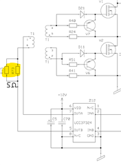
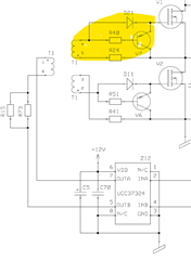
One of the issue is the switch on/off ringing of the FET output and the kind of weird looking driving voltage from the T1 transformer that is driving FET gate signals. It could be that the series resistors R15/R73 (22R resistors parallel) between T1 transformer and Z12 UCC373254 are there to slow down the GATE driving voltage. The issue which most likely comes from this is that the high side GATE driving voltage has glitches every now and then.

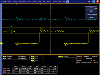
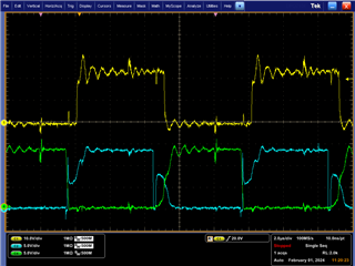
CH1 turn off/on waveform (yellow), CH2 T1 pin 6 (blue), CH4 V2 LOW side FET gate signal (green)

The other issue is the ringing after switch on and off that is not visible all the time, but most of.

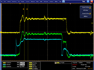
CH1 turn off/on waveform (yellow), CH2 T1 pin 6 (blue), CH4 V1 HIGH side FET gate signal (green)

Sometimes the driving signal looks well damped and it is not oscillating. I haven't really figured yet out what is causing this difference.

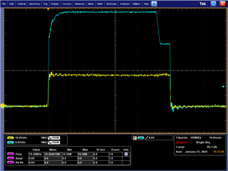
CH1 turn off/on waveform (yellow), CH2 V1 HIGH side FET gate (blue)

We have already tried couple of things.

  • smaller series resistors (was 11ohm -> changed to 5ohm) between T1 transformer and UCC37324 -> It slightly improved the glitches, but the glitches are still visible

  • Removed C86 and C27 100nF capacitors from FET outputs -> Little to no effect on the oscillation

  • added 470pF & 5ohm snubbers to FET bridge outputs -> Minimal improvement in FET oscillation
  • Tried also 820pF & 5ohm snubber combo on the V5 &V4 side, but that also had minimal effect on oscillation.

There are couple of things that I had in mind to still try. One is to modify the high side FET gate signal to slow down the switching on. The other one is to try different snubber components.

We are open to suggestion what to study/tune next.

  • Hello,

    Your inquiry is under review and I will get back to you shortly.

    Regards,

  • Hello,

    When it comes to passing irradiated emissions generally requires enclosing the design in a metal box that is grounded to earth ground and chassis ground.  This will help attenuate radiated noise from the power supply and will act as a Ferriday cage.  Does your design have this?  If not adding it may help reduce the radiated noise.

    To also help reduce the radiate noise from the line typically uses a common mode and differential mode input filter.  I do not see that on your schematic.  Adding these filter can help reduce and noise that is coupled from the design to the line.

    To reduce the power cord radiated noise.  Some designers have rapped the power cord in a ferrite toroid.  This will work as a common mode choke and will reduce noise on the power cord that could radiate.  Generally this toroid will be where the power cord exits the metal enclosure.

    Regards,

  • Hi Mike.

    Yes, this design is inside metal box. The metal box is grounded through 10nF capacitor to the input supply ground. I was told that since thist device is to be used in marine industry it can't be directly grounded. It was noted earlier that improving case grounding and board grounding did improve the emissions.

    And yes the schematic is lacking the input common mode coil. It is assembled just before the power supply lines exit the case. I don't know the original exact model, but we have tested the original common mode coil  (30mm diameter few turns of wire), Kemet SC-10-100 commonmode coil and Murata BNX016-01 model. There is slight difference between the three but these emissions are still visible with all of them. I will test also the power cord ferrite toroid.

    So you don't have anything to add to the schematic side or anything that I should test in that area?

  • For reference, a picture of the case and power supply cables


  • Hello,

    In your designs did you ground all of your heat sinks that were on switching nodes.  If not these heat sinks could act as antennas and cause you to fail EMI.

    Please note when doing this you generally need an insulation pads between the components and the heat sinks to prevent electrical shorts.

    Regards,

  • All the heatsinks are grounded to the case (with insulators in the components).

  • Hello,

    The next step would be to try to identify what part of the circuit the radiated EMI is coming from and try to shield it or remove it with snubbing if possible.

    Have you tried using a sniffer probe to identify noisy parts of your design? 

    Regards,

  • Hi. I think the closefield probe (HP 11941A) testing was done in the first testing phase. The main sources were L1 area on the left (amplifier output). L5, L6 and T3 area in the middle (+-180V switcher). And the input common mode filter area in the right (+24V input). And for your info, there are two amplifier & PSU boards in the device  and a CPU board that is driving those amps. Both of these amplifier boards have own powersupply cables but these boards are internally also connected together (J6 & J3).


  • Hello,

    In the beginning of this thread you had mentioned that you were failing Radiated Emissions.  Is the correct?

    Your EMI testing is done at 150 kHz to 30 MHz which is the range for Conducted Emissions.  Could you verify this please?

    Regards, 

  • Yes that is correct. The first picture is from our customer that made the testing. The radiated emissions have previously been measured at a frequency range between 150 kHz and 30 MHz where measurements are performed for magnetic (H) fields (CISPR 16-1 if I'm correct).

  • Hello,

    Are you sure these are not conducted emissions?   If they are conducted emissions you can solve them by adjusting the input filters.

    Specifications at 150 kHz measurement are generally conducted measurements.

    Could you double check this please?

    Regards,

  • I was just discussing yesterday with my collegue that we should do some more testing with conducted emissions measurement and different input filters.

  • Hello,

    I would start by increasing the X and Y caps to adjust the frequency poles (fp) of the filters.  fp = 1/(2*3.14*(L*C)^0.5))

    Remember these filters should decrease the noise by -4dB per decade after fp.

    Give that a try and let me know if it works out for you.

    Regards,

  • Hi. Been busy with other projects, but had now time to look this again. Where would you mount the X and Y-capacitors? Over the T3 transformer?

    I had good results in another project with PI-filter in the input and decided to try it  here also after CM-coil (between CM-coil and FET-bridge). I used 100µF cap parallel, 5.6µH inductor and 150µF capacitor parallel after the inductor. For some reason this had minimal effect on the 100kHz harmonics when measuring conducted measurement from the power cable. 

  • Hello,

    The X and Y capacitors are generally put across the common mode and differential mode input filters.  The following filter will bring you to a presentation on EMI filtering.  This should help you setup your EMI filter with the X and Y capacitors.

    file:///C:/Users/a0799388/Downloads/Bing%20Lu_Introduction%20to%20EMI%20in%20power%20supply%20designs.pdf

    When it comes to filtering it is just not the capacitance that make the difference it is also the inductance.  Remember the double pole for a filter is fp = 1/(2*3.14*(L*C)^0.5).  So with one filter you had a good response with a certain capacitor it may not work with a different filter or with inductance.

    The double pole filters bot common mode and differential mode should have there poles set at least a decade before the noise they are trying to attenuate.

    Regards,