This thread has been locked.

If you have a related question, please click the "Ask a related question" button in the top right corner. The newly created question will be automatically linked to this question.

BQ76940: DSG MOSFETs getting damaged during SCD.

Part Number: BQ76940

Hello experts,

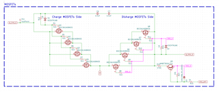
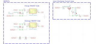
I am having a problem with the MOSFETs getting damaged when we do SCD. We have designed two boards as potential fixes for this problem. Board A has 4 N Channel FETs in parallel on each CHG and DSG side (MPN: BSC061N08NS5) and Board 2 with a single N channel FET each on CHG and DSG side. (MPN: PSMN1R9-80SSEJ). The pack is 14S14P configuration with Panasonic 18650BD as cells.

Board A Schematic:

Board B Schematic:

AFE Schematic from the BMS logic board:


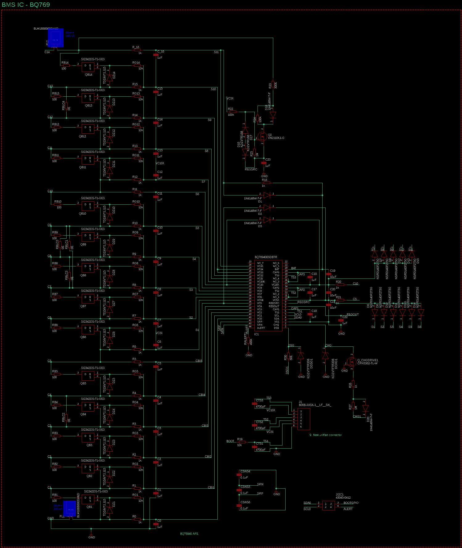
We know that the AFE is detecting the SCD as we see the SCD alert flag being raised and our MCU controller being able to see and log the event. Based on suggestions from BQ769x2 app note, we have also added a local PNP turn off circuit to help dissipate the parasitic gate capacitance that the MOSFETs might have. With all these changes we are still failing SCD. The DSG MOSFETs are blowing apart and shows a short between source and drain.

As we had smaller test packs made we also tested with that. Here are the results.

  1. Board A - 14S1P - Cleared.
  2. Board A - 14S10P - Failed.
  3. Board A - 14S14P - Failed.
  4. Board B - 14S1P - Cleared.
  5. Board B - 14S10P - Cleared.
  6. Board B - 14S14P - Failed.

This makes me think the avalanche current rating of the MOSFET is the parameter that is making the difference because with the cells in parallel reducing the max current the pack can reach in a short also reduces. I also want to discuss the idea of adding a gate driver IC or even use a Battery Gauge from TIs portfolio as these devices are more equipped to handle large MOSFETs.


I will edit the post and keep adding more relevant information as the I do further tests. Please project your thoughts.

Best,
Abhijith.

  • Hi Abhijith,

    One of the most common sources of FET damage that we see during SCD testing is that the switching speed of the FETs is either too fast or too slow.

    This FAQ goes more in depth on the matter (link), and I recommend reading it over to apply to your testing.

    Also, R12 and R13 are recommended to be 10M.

    Regards,

    Max Verboncoeur

  • Hello Maxwell,

    • I have seen this post earlier and have considered that during the design.
    1. Like I mentioned, point 1 in the post is not the issue because I am able to see the flag raised by t-he AFE on my logs.
    2. Point 2, for faster turn off I have added the local path using a PNP MOSFET as shown in Figure 8-21 of Multiple FETs with the BQ769x2 Battery Monitors
    3. Point 3, I have 1k (R15) in series with individual gate resistors (51E). So I think this should be enough to NOT turn it on very fast. Please tell me if I am wrong. 
    4. I think the gate resistors should be able to fairly damp the oscillation. And Board B has a single MOSFET anyway. So oscillation shouldn't be a problem.

    Hence I wrote this post for further help in the matter. Can you please get  or someone from your expert team get on this? As you guys might have seen many designs used by customers and would've designed many boards yourselves, I'd like to know what is generally followed.

    • R12 and R13 should be 10M? On the EVM I see they have used 10k/1k itself. I think you have misread the ref designator. Can you please check again?
    • Can you also tell me or link to me something that can explain how the SCD setting in the device works? I would like to know this in detail.

      Thanks,
      Abhijith.
  • Hi Abhijith,

    Point 3, I have 1k (R15) in series with individual gate resistors (51E). So I think this should be enough to NOT turn it on very fast. Please tell me if I am wrong. 

    Point 3 of the FAQ is that the FETs turn off too quickly, which could be the root cause of your case. You may be able to get a better idea of what is happening on a scope.

    Can you also tell me or link to me something that can explain how the SCD setting in the device works? I would like to know this in detail.

    Section 8.3.1.2.1 of the datasheet contains an explanation of how the SCD protection functions, though in short, it is implemented using a voltage comparator between the SRP and SRN pins.

    Regards,

    Max Verboncoeur

  • Hello Maxwell,

    Yes, it was a typing mistake I made. I meant to say the 1k + 51E that on the line from the DSG signal of the AFE will provide enough resistance to prevent the MOSFETs from turning off very quickly. So I also have a fix for this. I will try increasing the gate resistor value from 51E to something like 470E. I will also put a scope on the line and try to get more clarity. Will write back with the results. In the meantime can you check for anything apart from this?

    I will look into the SCD section.

    Best,
    Abhijith.

  • Hi Abhijith,

    I think it is most likely that the BJT current loop is turning the FET off too quickly. Increasing the resistor on the collector would help to control the speed of the turn off.

    Again, sharing a waveform of the FET turn off would help to determine if this is the case.

    Regards,

    Max Verboncoeur