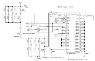
This thread has been locked.

If you have a related question, please click the "Ask a related question" button in the top right corner. The newly created question will be automatically linked to this question.

TPS53319: Eliminate Radiated Emission

Part Number: TPS53319

Hi,

TPS53319 is being used to generate 3V3 from 18V on our custom board (the schematics screenshot is attached). The product is failing in CISPR32 Class B radiated emission test (at 3m distance) in 35MHz to 46MHz range. On probing with near filed probes and spectrum analyser, we could find some emission from near the TPS53319 device. Ripples of 250mV is also observed on the 3V3 output.

Kindly check and suggest solution(s) to eliminate the radiations.

Regards,

Thariq C P

  •  

    Emissions in the 35-46MHz region are generally going to be coming from the resonance of the switching node (LL pins) which is rapidly switching between 0V and 18V while carrying the loading current.

    Unfortunately, your existing schematic does not appear to include the components we normally use to mitigate this noise.

    1) An 0402 capacitor placed close VIN and GND (exposed pad) with the lowest possible series inductance can be effective at reducing the energy.  Measure the frequency of ringing at the switching node and select a capacitor whose self-resonance frequency is as close to the ringing frequency as possible.  For 35-46MHz, I would look at 10nF to 47nF capacitors in an 0402 package.  These capacitors typically have an ESR in the 100-400mOhms range and are self-damping.

    2) Adding a 1-4.7Ω resistor in series with C525 will slow down the turn-on of the high-side FET, which will also reduce the energy stimulating the resonance to reduce the ringing.  The higher the resistance, the more it is reduced.  Going higher than 4.7Ω can cause the high-side driver to "pinch off" and introduce additional issues, so that should be avoided.

    3) An R-C snubber from LL to GND can help absorb and dissipate any resonant energy generated at the switching node.  Typically capacitor values are in the 1-4.7nF range and resistors in the 1-3.3Ω.  The optimum values depend on layout parasitics such as capacitance and inductance.  I am attaching a spreadsheet that can guide you through measurements and optimizing the values.

    2642.Snubber_Calculations.xlsx

    4) Since the strength of radiated emissions at 3m is going to depend on the antenna size on the board carrying the energy, containing the energy to the smallest possible area will also help.  This will obviously require some layout considerations at the TPS53319.

    1. Keep the area of the switching node (LL pins to Inductor) as small as practical.  Avoid sharp corners like 90 degrees.  Chamfer at 45 degrees or round corners whenever possible.
    2. The LL net should over the inductor terminal but should not extend past the inductor terminal.
    3. The LL net should not be any close to VOUT than the inductor terminals to avoid increasing capacitive coupling between LL and VOUT.
    4. If there is GND net close to the LL net, especially if there is GND under the inductor it must be stitched to the GND plane with an array of vias.  A "floating" ground with long traces to the nearest vias to the ground plane will serve as a conductor for high-frequency noise rather than a shield.
    5. Adding a couple of 0402 ceramic capacitors right at the VOUT terminal of the inductor with self-resonance frequency matched to the LL resonance frequency will help conduct that noise immediately back to ground to minimize radiation antenna area.
    6. Output capacitor layout where VOUT flows between capacitors with ground on either side and multiple vias to ground planes will also help reduce high-frequency impedance at the VOUT net and conduct high-frequency noise to ground for improved performance.

    Hopefully that should give you direction on how you can improve your radiated emissions.

  •  

    I forgot to mention, because the power dissipated in the snubber resistor is Csnub x Vin^2 x Fsw, for 18V input and 500kHz, each nF of Snubber capacitance is going to dissipate 162mW of power, so you will need a larger resistor pacakge, possibly multiple resistors to dissipate the snubber energy.