This thread has been locked.

If you have a related question, please click the "Ask a related question" button in the top right corner. The newly created question will be automatically linked to this question.

TPS6593-Q1: WD_PWRHOLD not set when DISABLE_WDOG pin is set

Part Number: TPS6593-Q1

Dear forum,

according to the device documentation "Device sets WD_PWRHOLD if hardware condition on pin DISABLE_WDOG (mapped to GPIO8 pin) is applied at start-up".
Unfortunately this is not working on our system.

After power-up we check via I2C from the u-boot bootloader:

  • Read register "GPIO8_CONF" offset 0x38 to ensure GPIO8 is configured as DISABLE_WDOG input pin

    => i2c dev 1                   ---> 3 = Pin configured as DISABLE_WDOG
    Setting bus to 1               |||     
    => i2c md 48 38.1 01           7654 3210
    0038: 6a    j               -> 0110 1010

  • Read status of GPIO8 via register "GPIO_IN" offset 0x3F reflecting high state of DISABLE_WDOG

    => i2c dev 1                   -> GPIO8
    Setting bus to 1               |
    => i2c md 48 3F.1 01           7654 3210
    003f: dc    .               -> 1101 1100

  • Read WD_PWRHOLD via register "WD_MODE_REG" offset 0x406 which is unexpectedly 0 (should be 1 as DISABLE_WDOG is high) 

    => i2c dev 0                         -> WD_PWRHOLD (Why not 1??)
    Setting bus to 0                     |
    => i2c md 12 406.1 01          7654 3210
    0406: 02    .               -> 0000 0010

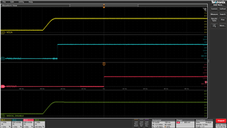
Please find below the oscilloscope capture of WDOG_DISABLE and nRSTOUT (MCU_PORz) during power on. There is roughly 20 mS of time duration of WDOG_DISABLE set high before nRSTOUT goes high. This fulfills the 30 uS requirement of tWD_DIS (DISABLE_WDOG input signal deglitch time).

For a more complete PMIC register view please find below the registers (just after power up) from I2C address 0x12:

=> i2c md 12 0.1 0b
0000: 00 00 3c 7f 7f ff 02 0a 00 bf 00 ..<........

...and the registers from I2C address 0x48:

=> pmic dev pmic@48
dev: 1 @ pmic@48

=> pmic dump
Dump pmic: pmic@48 registers

0x00: 00 9a 11 05 33 2b 22 2b 32 28 31 2b 31 1b 2d 2d
0x10: 2d 2d fd fd 73 73 b2 b2 1b 1b 1b 24 24 22 02 33
0x20: 33 00 00 f4 38 12 38 24 24 24 24 20 7f 00 00 00
0x30: 00 20 40 ba 01 1a 18 2a 6a 1a 1a 1a 19 08 00 dc
0x40: 08 55 75 01 2d 01 55 50 00 00 00 00 00 00 00 ff
0x50: ff 3f 11 02 30 00 00 01 08 07 10 00 00 00 00 00
0x60: 00 00 00 00 00 00 01 00 00 00 00 00 00 00 00 00
0x70: 00 00 00 02 00 00 00 00 55 01 55 99 00 43 00 00
0x80: 00 09 02 00 0f 00 00 00 00 00 00 0b ff ff 00 00
0x90: 00 00 00 00 00 00 00 00 00 00 00 00 00 00 00 00
0xa0: 00 00 00 80 00 00 08 00 00 00 00 00 00 00 00 00
0xb0: 00 00 00 00 00 00 00 00 01 01 00 00 00 00 00 00
0xc0: 00 00 00 e0 80 00 00 00 00 00 00 00 00 00 00 00

What reason could cause WD_PWRHOLD not to be set as expected?

Thank you and best regards, 
G. Friedrich

  • Hello Götz,

    Please allow some time for us to look over this post and thank you for the register dump.

    My apologies on that, but you're right the expected behavior is to have the powerhold high, but these register reads, when were they done, before or after the enable pin has been set to logical high?

    BR,

    Nicholas

  • Hello Nicolas,

    aus you can see from the oscilloscope trace the WDOG_DISABLE pin is directly set to logical high when powering up the device. With that all register reads are done when the pin is already at logical high.

    BR, Götz

  • Götz,

    Just trying to confirm as nothing seems out of the ordinary, but the WD PWRHOLD not setting to one.

    As the program for each one of the TPS6593 devices are highly configurable a static register dump doesn't tell me what happens during transitions between states.

    Do you have part number on hand for this device or did you program the PFSM yourself?

    BR,

    Nicholas

  • Hello Nicholas,

    thank you for your support The part number is TPS65931211RWERQ1 (device print shows: TPS6593 1211-Q1 TI 3AG M08J G4) which we did not program by our own.
    As you can see from above register dump...

    NVM_CODE_1 = 0x11
    NVM_CODE_2 = 0x05

    ...which corresponds to https://www.ti.com/lit/ug/slvucm3/slvucm3.pdf section 5.2 Device Identification Settings

    -Best regards, Götz-

  • Hi Götz,

    US has a public holiday today February 19th so Nicholas will get to you in the next few days. Thank you for your patience.

    regards,

    Niko

  • Hello Niko,

    thank you for the feedback! Please let us know if there are open questions.

    -Best regards, Götz-

  • Hello Götz,

    While it does say that in the datasheet. This is only partially true.

    As it's need to be up before the device transitions into the PFSM, typically customers have this pulled up to VCCA via a resistor.

    Would it be possible for you to do this or take a oscilloscope shot of VCCA, ENABLE, & GPIO8.

    Thank you & BR,

    Nicholas

  • Hello Nicholas,

    thank you for your reply and sorry for the late answer. We are working on that topic and need some more time for the measurement. We will come back to you as soon we have the results.

    -Best regards, Götz-

  • Hello Götz,

    thank you I appreciate this.

    BR,

    Nicholas

  • Hello Nicholas,

    as suggested we pulled-up WD_DISABLE (GPIO8) to VCCA with a 10 kOhm resistor:

    It seems like this made no change to the PMIC registers:

    => i2c md 12 0.1 0b
    0000: 00 00 3c 7f 7f ff 02 0a 00 bf 00 ..<........

    => pmic dev pmic@48
    dev: 1 @ pmic@48

    => pmic dump
    Dump pmic: pmic@48 registers

    0x00: 00 9a 11 05 33 2b 22 2b 32 28 31 2b 31 1b 2d 2d
    0x10: 2d 2d fd fd 73 73 b2 b2 1b 1b 1b 24 24 22 02 33
    0x20: 33 00 00 f4 38 12 38 24 24 24 24 20 7f 00 00 00
    0x30: 00 20 40 ba 01 1a 18 2a 6a 1a 1a 1a 19 08 00 dc
    0x40: 08 55 75 01 2d 01 55 50 00 00 00 00 00 00 00 ff
    0x50: ff 3f 11 02 30 00 00 01 08 07 10 00 00 00 00 00
    0x60: 00 00 00 00 00 00 01 00 00 00 00 00 00 00 00 00
    0x70: 00 00 00 02 00 00 00 00 55 01 55 99 00 43 00 00
    0x80: 00 09 02 00 0f 00 00 00 00 00 00 0b ff ff 00 00
    0x90: 00 00 00 00 00 00 00 00 00 00 00 00 00 00 00 00
    0xa0: 00 00 00 80 00 00 08 00 00 00 00 00 00 00 00 00
    0xb0: 00 00 00 00 00 00 00 00 01 01 00 00 00 00 00 00
    0xc0: 00 00 00 e0 80 00 00 00 00 00 00 00 00 00 00 00

    -Best regards, Götz-

  • Hello Götz,

    this is quite strange. I understand the question. I'll be speaking to my team members on this, I have used an EVM in order to replicate the issue, but I am unable to do so.

    BR,

    Nicholas

  • Hello Nicholas, 

    do you have any feedback from your team?

    -Best regards, Götz-

  • Hello Nicholas, a small reminder reg. that topic. BR, Götz

  • Götz,

    I have been trying to recreate your issue on EVM, with 5V input and the separate power supplies for the proper boot sequence.

    The watchdog power holds works as expected and have not been able to recreate this issue. I know this may seem silly, but where on the board are you probing?

    In the schematic and I can't see the network, so please double check this probe.

    The logic is hard tied to the device that input voltage raising with VCCA to 5V should be enough as the threshold to turn on all internal logic ~2V75 and the threshold for logic high on GPIO8 being ~1V26.

    BR,

    Nicholas

  • Hello Nicholas,

    I am a colleague of Götz. The signals were measured at test points that we included on our board:

    VCCA: TP11
    PMIC_ENABLE: TP30
    NRSTOUT: TP45
    WDOG_DISABLE: TP41

    All test points can be found in the schematics excerpt we sent you via E-Mail.

    I also tried to reproduce the behavior on the AM62A EVM which has the same PMIC installed. The PMIC on the EVM behaves as described in the datasheet.

    One difference I noticed between the PMIC on the EVM and the PMIC on our custom board is the register value TI_NVM_REV. On the EVM, TI_NVM_REV is 2, on our board TI_NVM_REV is 5.

    What are the differences between these revisions?

    Best regards,
    Pascal

  • Hello Pascal,

    What are the differences between these revisions?

    The biggest difference is highlighted below, and it has to do with the GPIO6 input for switching voltage on the core.

    On the left is the rev5, rev3 on the right.

    Nothing about GPIO8 or the watchdog is changed between any of the versions.

    BR,

    Nicholas