This thread has been locked.

If you have a related question, please click the "Ask a related question" button in the top right corner. The newly created question will be automatically linked to this question.

TPS922055DMTREVM: How to optimize the SW pin output waveform?

Part Number: TPS922055DMTREVM
Other Parts Discussed in Thread: TPS922055

Hi Team,

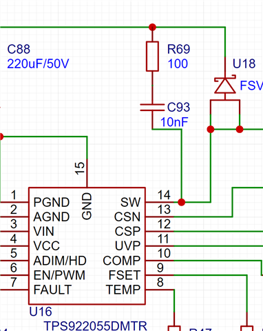
Use TPS922055 driver LED lamp, 36V power, output voltage 20-25V, current 3.5A.

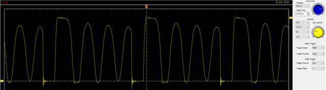
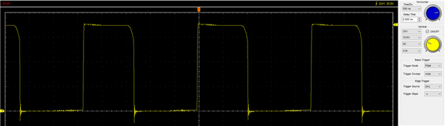
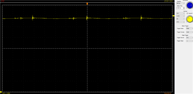
Use the oscilloscope to check the chip 14 pin SW, when the PWM is less than 10%, the output waveform interference is large (PWM is more than 20% waveform is better).

Double-sided circuit board design.

There are two sets of independent output circuits on a circuit board.

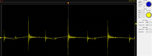
36V power waveform also has large interference, how to improve?

The schematic diagram is as follows:

SW waveform diagram is as follows: (@10%PWM)

SW waveform diagram is as follows: (@20%PWM)

36V power waveform diagram is as follows:

Best Regards,

Kevin

  • The pictures is not clear. Send it again

  • 1.Reference TPS92205xEVM design, but PGND and AGND are not separated and directly connected together.

    2.The frequency of the input PWM signal on the ADIM/HD pin is 20kHz, and the PWM duty cycle corresponds to the current linearity,

    3.The SW pin waveform is good when the PWM duty cycle exceeds 15%

    4.The current waveform cannot be measured without a measuring probe. Only a multimeter can be used to measure current.

    5.Does adding C89 and C90 to the output reduce interference?

    6.How can improvements be made to reduce EMI?

  • Hi Kevin,

    1. What do you mean by interference? Do you mean input / output voltage ripple?

    2. When the PWM duty into the ADIM/HD pin is low, the system will enter into discontinuous conduction mode and that's the reason why you see oscillation when PWM duty = 10%.

    3. There are many things and common techniques you can use to reduce EMI. For example, you can use an RC snubber to damp the oscillation when the internal FET turns on.

    Best Regards,

    Steven

  • Hi, Steven

    1.Yes,I want to reduce the output voltage ripple.

    2.There is a large voltage ripple between the inductance and the sampling resistance.(L6 , R3)

    3.Increase the RC snubber (R69, C93) as shown below?

    4. The C69 and C72 are not in the reference design of DataSheet, but are in TPS92205xEVM . Is this necessary ?  Need to replace C72 with a 1M resistor?

    5.Is it better to reduce power ripple by separating PGND and AGND?

    Thanks

    Best Regards,

    Kevin

  • Hi Kevin,

    1. Understood.

    2. Adding some some-value capacitance like 100nF to the output capacitor may help reduce the high-frequency noise shown above. Enlarging the inductor / switching frequency can help reduce the low-frequency noise (the switching ripple).

    3. Yes. This is the correct position for the RC snubber.

    4. C69 and C77 is not needed. This FAQ can give you some idea on how to design the COMP pin components - [FAQ] How to design the COMP pin components for TPS922055 / TPS922054 / TPS922053 / TPS922052?

    5. I do not think the PGND/AGND connection is the main cause of the ripple based on the current information you provide. Please try No.2 suggestions first and see if it helps. 

    Best Regards,

    Steven

  • Hi Steven,

    Thanks, I will test it according to your suggestion.

     If i add a capacitor between the output and the ground, will the voltage ripple be reduced?

    Best Regards,

    Steven

  • Hi Kevin,

    Do you mean adding a capacitor between LED cathode and GND? If so, then this is not a common method that we use.

    Best Regards,

    Steven

  • Hi Steven,

    Thanks for answering my question. Thanks again.

    Best Regards,

    Kevin

  • Hi Kevin,

    You are welcome. Please let me know if you have any further question.

    Best Regards,

    Steven