A related question is a question created from another question. When the related question is created, it will be automatically linked to the original question.
If you have a related question, please click the "Ask a related question" button in the top right corner. The newly created question will be automatically linked to this question.
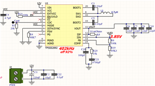
After inspection turns out it was bad solder joint across enable, it was shorted to gnd. Output is working now, on set voltage. But another thing is now popped. Circuit current increase in 1min to draw 200mA on idle open output. Is it problem with F settings for this input/output range 12V/3.8V? Now is around 400kHz.
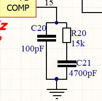
I think the large output voltage ripple is due to unsuitable compensation parameters, please try to change R20=3.9k, C21=8.2nF.
And the input current is about tens mA level at FPWM mode with no load when you connect MODE to VCC, because the internal MOSFETs keep switching at every cycle to obtain small output voltage ripple. If you need smaller input current, it is recommend to select PFM mode by connecting MODE pin to GND, but the disadvantage is higher output voltage ripple.
Hi Bryce, it's perfect with you suggested values. 92% eff for my case 12Vin, and 3.9Vout 2A. 20mA at idle no load state.This is signal on open load. Ripple while load is less than 50mV.