This thread has been locked.

If you have a related question, please click the "Ask a related question" button in the top right corner. The newly created question will be automatically linked to this question.

LM25148: Stubborn Instability of typical application circuit

Part Number: LM25148
Other Parts Discussed in Thread: INA280

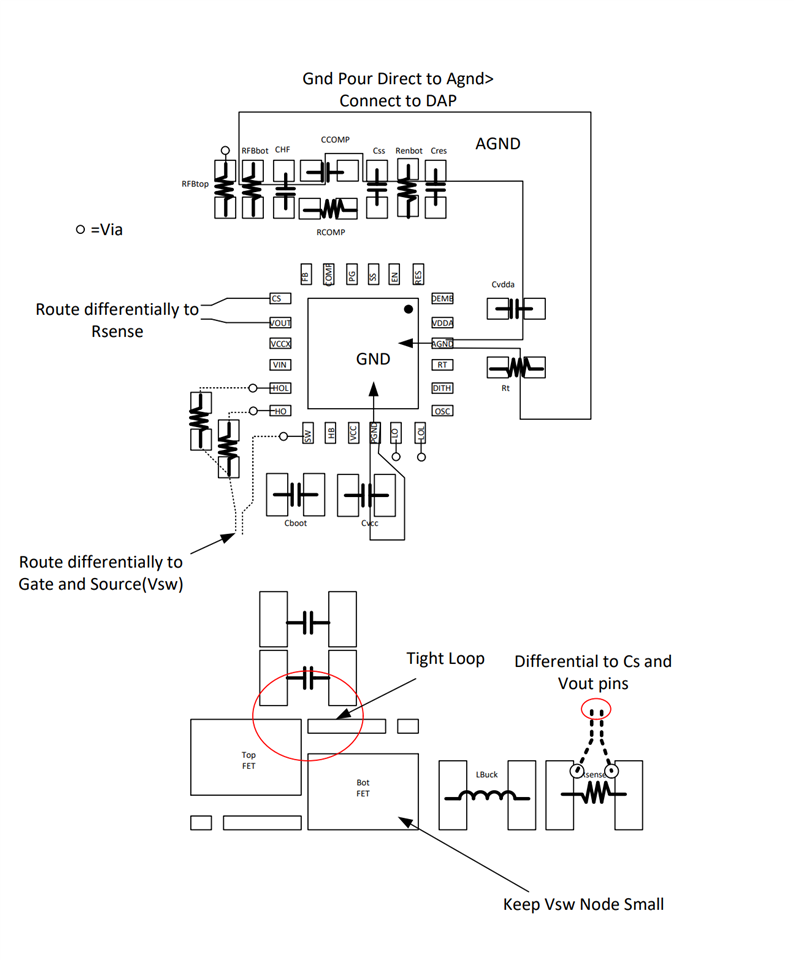
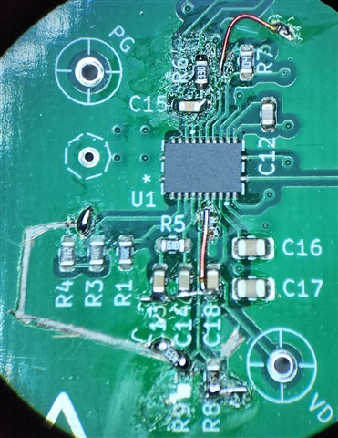
I am developing a power converter based on the LM25148. My first design was not stable and I could not diagnose the problem so I backed up to the typical design #2 in the datasheet. I recreated the design using nearly identical parts and closely copied the layout from the LM25149EVM. See the schematic below:

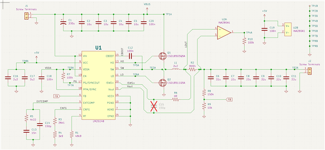
The only change I made from the reference design was increasing the output voltage from 5V to 12.8V. I increased the voltage rating of the output capacitors accordingly. The INA280 was supposed to measure the inductor current for troubleshooting but may have been a poor choice due to bandwidth and saturation limits. 

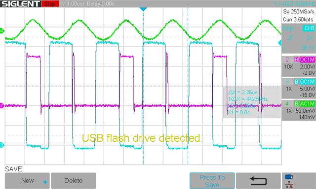
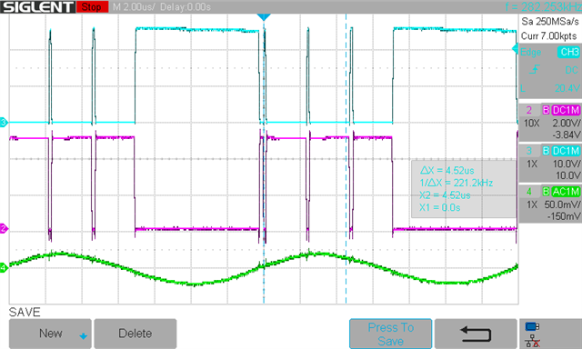
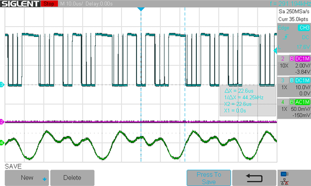
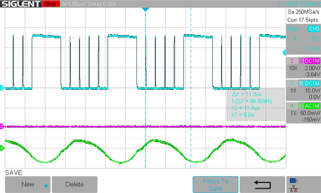
At loads above ~3.5A I begin to see inconsistent switching as demonstrated in the scope shot below. The blue trace is the SW node and the green trace is Vout. 

Longer pulses are followed by shorter pulses (the smaller pulse width looks like minimum on time). 

This behavior is load dependent and exhibits some hysteresis when the load increases and decreases. More specifically the instability will begin at a certain increasing load, and remain even when the load drops below the draw when the problem began. 

I have used the TI design calculator to check my design, I should have a more than adequate 78 degree phase margin and a -18dB gain margin. I have taken the following steps to fix my problem:

1. Add a filter to the ISNS+ and Vout pins as used in the EVM

2. Adjust my compensation network to account for inaccuracies in my overall transfer function analysis 

3. Purchase and test the TI produced EVM to rule out test equipment problems

The EVM from TI seems to work fine and rule out my test equipment as a problem, though there are always possible edge cases. I have taken other steps to troubleshoot the device such as various filter and configuration adjustments, but these changes did not help and I did not document them well. 

I feel like I am slightly losing my mind as I cannot see why the EVM works but my design does not. I can supply layout files and any other scope shots if that will help. 

  • Hello Liam,

    Can you fill out design calculator detailing your spec so I can check your schematic against the calculator results.

    Thanks.

    David.

  • Hello David, Find attached. There definitely may be a nuance I'm missing. It's also worth noting that I thought I'd solved the problem after looking at TI literature SLUP 384 section VI. But adjusting my compensation network dd not seem to change the behavior I was observing. 

     LM25148_LiamCRaig_forumcopy.xlsm

  • Thanks Liam,

    Can you change the Lbuck to 6.2uH and retry, I think this may help.

    Hope this helps.

    David.

  • Thank you for the suggestion David. I did not have a 6.2uH inductor of the correct size at hand so I tried a 5.6uH and an 8.2uH. The same behavior is occurring and actually occurring at lower load currents. Did you make this suggestion due to the inductor ripple calculation? I also found the inductor value in the reference design to be suspiciously low but I wanted to start from a known working design. That has unfortunately not played out so simply. 

    I should also say I've built up a second design with different power path components that exhibits similar behavior. I'll leave that out of this conversation for now as I think that's another can of worms. But we have additional hardware to compare to. 

  • Possibly an additional hint, see this scope shot of the SW node (blue) and the LO driver signal (pink). This is at a lower load current than the inconsistent SW behavior. The SW node high looks consistent but the LO drive seems to be alternating.


  • Hello Liam,

    This is a peak current mode device, and I was making the suggestion of Lbuck because inductor selection is important for the current loop to avoid sub harmonic oscillations.  you latest waveforms are interesting, showing the LS gate drive is current off like the Zero cross detect circuit is cutting in.  the switch node looks stable at this point.      Can you do me a favor and cut PFM to VDDA and pull to Gnd for FPWM operation, is everything stable then?

    Thanks.

    David.

  • Thanks David, 

    First of all, thank you for your help and your patience. It took me a little time to implement that bodge and take new measurements. 

    The bad news: the short pulses are still present and there are now always two short pulses after a large pulse. see below. From top to bottom the waveforms are SW, LO, and Vout.

    The good? news: this behavior is now at least consistent. the waveform looks like this through the entire load range (0-5A). 

    If it would be at all helpful please reference my schematic to see where I've included test points (TP*). I can measure those points with extreme ease and provide you with waveforms.

  • Thanks Liam,

    OK, that kind of points to a stability issue.  Can be due to noise, let's check your layout.  can you tell me if you followed this conceptual layout?  this concept is acutally for a similar part, but the approach is exactly the same.

    NOTES

    CIN cap close to HS/LS FET with a tight loop.

    Differential routing of HS gate drive.

    Diff LS Gate drive, but if you have a Gnd plane on an inner layout its default differential...

    Differential routing of CS back to the IC.

    VCC, Cboot close to IC.

    Analog Gnd pour stitched single point back to the devices DAP where it Meets power Gnd.

    Hope this helps.

    David.

  • Thank you David, I have definitely followed most of these practices but I did not separate the analog ground. It is possible but significantly time consuming for me to carve out the analog ground from the rest of the ground plane. I'll get to it with the scalpel and microscope.

    Depending on your location I imagine you are signing off soon so I may not complete the modifications before your end of day. I will bring detailed results back to this thread for discussion whenever you are back at it. 

  • Thanks Liam,

    Looking forward to an update.

    Thanks

    David.

  • Hi Again David, 

    I managed to improve the grounding scheme but I was not able to make the single connection occur at the DAP. I connected the planes nearby but I did not see improved behavior. I fear this grounding could still be an issue.

    I did get some interesting scope shots, this first one shows that there is (probably) subharmonic oscillation on Vout. (blue SW green Vout)

    The picture above has multiple  frequencies in the output ripple and shows variation in the wide pulses as well. Under most load conditions there is only one ripple frequency as shown below.

    I'm not sure if this is more indicative of noise or improper compensation. 

    I don't think there's any way to avoid a new layout at this point. I am working on it now and plan to post some side-by-side comparisons of my changes here. There's only one thing I'd like clarification on for your layout recommendations.

    When you are talking about differential routing of the gate drivers, I want to tightly couple the gate and source right? So for the high side driver I want HO and SW tightly coupled between the LM25148 and the high FET, and for the low side drive I want LO and ground coupled tightly between controller and low FET.  Should the SW trace and LO be spatially separated? I'm just unsure if EM coupling between LO drive and SW is good or bad in this case. 

    Much Thanks, 

    Liam

  • I've closely re-read the datasheet layout section and it answered my last question. Please feel free to ignore that

  • Hello Liam,

    I think it may well be your layout causing the issue.  I think making another layout and following the suggestion will resolve your issues.

    Hope this helps.

    David.

  • It seems like the best thing to improve right now anyway. Thank you for all your help I'll close this thread and open a new one if I have similar problems with an improved layout.