This thread has been locked.

If you have a related question, please click the "Ask a related question" button in the top right corner. The newly created question will be automatically linked to this question.

UCC28C50-Q1: UCC28C50 Flyback PSR startup and regulation

Part Number: UCC28C50-Q1
Other Parts Discussed in Thread: UCC28C50,

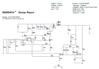
Starting from these Flyback PSR and SSR Webench designs:
webench.ti.com/.../SDP.cgi

 I've just buld up 2  build up 2 circuits using a custom multiout transformer.
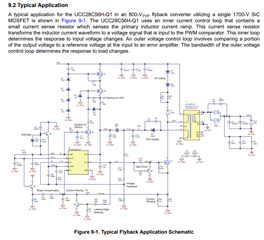
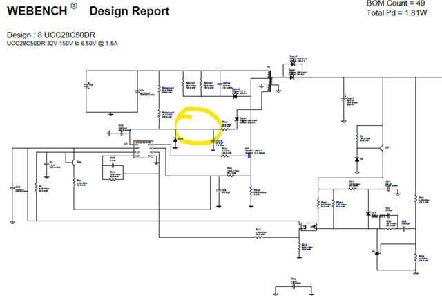
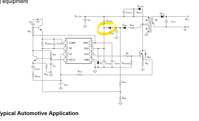
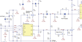
While the SSR circuit seems to startup and regulate properly, the PSR does not start.  The cirscuis is the following and replicates the Webench design:

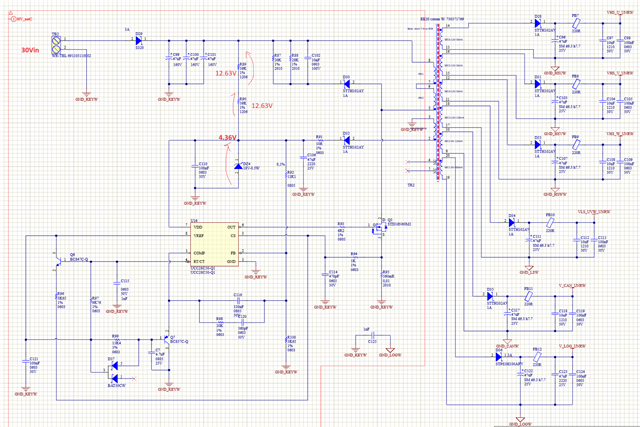
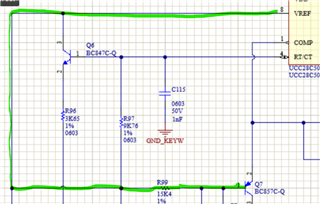
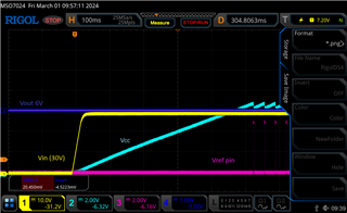
Doing some measures @30Vin I noticed that voltage at Vdd pin7 UCC28C50 stays a lot below it's Vddon threshold (4.36V as pointed out on schematic).
Stayin below 30Vin I could startup the IC just bypassing for a short time the 2 startup resistors R89-R90 seeing the oscillation start of the controller and the Vouts at no load. Applying a minimal load however, outs drops without anuy regualtion.
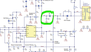
I have the doubt that the generated Webench PSR schematic is correct?  In my opinion there's should be a decupling diode beetween the startup resistors and the rectified voltage coming from the primanry auxiliaty winding...

  • Hi Flavio,

    -I can not see the webench design recommendation from the links that you shared.

    -Looking at your schematic, I noticed:

    1. RT/CT: RT resistor is not placed and connected. RT needs to be connected between VREF and RT/CT pin to charge CT cap during the on time.

    2. Soft start: the base of Q7 should be connected to VREF through R99. It is connected to COM pin in your schematic. Be aware that BAT30CW is floating.

    3. Slope Compensation: I recommend connecting a capacitor in series with R96. Please, check Section 9.2.2.13 that suggest design value.

    4. Rstart: Start up resistors must be designed considering a typical start-up current at VDD pin of 75uA (UCC5x...) and UVLO.

    I recommend following the Datasheet Criteria Design (Section 9) if you have any doubts with your components selection

    Thank you.

  • Thank you Manuel,
    here the webench report generated from to the missing link above:
    5751.WBDesign8_PSR_NoOpto.pdf

    About your notes:
    1- Rt is representedi by R97 and CT by C115 as in the webench report
    2- Base of Q7 connected to Vref through R99:

    3-Ok for adding a cap in series of R96. Noticed however that I 've also tries to disable the slope compensation (opening R96) with no results.
    4- Values fo Rstart have the same values of the Webench report (78K total) to impress a Vdd current >75uA in fact. As suggested in the Typical Flyback Application you mention

    I tried to insert a decupling diode+cap between the voltage feedback path and UCC5x Vdd pin (non however present on generated report)  with no  results (ie the IC does not start).

    Looking forward to hearing from you, kind regards

    flavio

  • Hi Flavio. Will be back to you tomorrow afternoon. Thank you

  • Hi Flavio. For a better debug, please show Startup single shot waveforms of (VIN-GND), (VDD-GND), (COMP-GND), (VOUT-GNDS) in an oscilloscope. We need to check if VDD is triggering UVLO and/or it is in Fault mode. You can check the startup waveforms of the UCC28C50's User Guide Section 5 Performance Data, so you have an idea of the amplitude and time scales for the waveforms (see below). Please, note that GND (primary ground) and GNDS (secondary ground) are different ground references, as the secondary side is isolated from the primary side.

    User Guide: UCC28C50's User Guide

    Thank you

  • Hi Manuel. Here attached my waveforms screenshot at startup.
    Ch1 (jellow) : input voltage
    Ch2 (cyan): Vcc (pin 7 UCC28C50
    Ch3 (Magenta): Vref out pin UCC28C50
    Ch4 (putple): Vout (secondary out got via differential probe)

    Furthermore:
    - Vref signals pulses (30ms period approx) and Vcc never goes over the start threshold of the chip (7V typ)
    - I noticed that the Vcomp signal remaning stationary (not seen on screenshot)
    - introduced a 1uF cap on the slope compensation network (in series with R96)

    I'm wondering: Is the generated Webench circuit correct?

    thanks

    flavio

  • Hi Flavio.

    Thank you for the waveforms. UCC28C50 is in Fault mode according to VCC waveforms (ramping up and down UVLO ON/OFF).

    I have a question regarding Vout waveform: Why does it show a 6V constant values during the entire time length? Vout is supposed to ramp up from 0V up to the setpoint desired value (6.5V). Is the output capacitor pre-biased/pre-charged? Please, make sure that Vout is 0V when the power supply (Flyback) is OFF. You can place a high resistor value (10Kohm) to discharge the cap when the power supply is off, or you can gently/carefully shorted when the power supply is OFF. 

    Looking at the WEBENCH report, the schematic was design to provide power to a single output 6.5V@1.5A (9.75W). In your actual schematic, I can see that there are multiple output windings, is the power spread? What are the load conditions of each output?

    Please confirm that this is the transformer your are using:

    It might be that VIN=30V is not high enough to turn on the device, is it starting at higher VIN values?

    Now that Fault mode is confirmed, if the startup problem persist, we need to check your (DRV-GND), (CS-GND), (COMP-GND) (VCC-GND) and (VOUT-GNDS) waveforms to see what kind of fault is being triggered in the device and then we can address the solution. If your scope has just 4 channels, skip (VOUT-GNDS). When taking the single shots, check the best scale for all the waveforms to be able to see all of them. Always select the trigger on (VCC-GND) cannel, rising UVLO ON.

    Thank you.

  • HI Manuel,
    answers to your questions are the following:
    1- Vout is still low 0V (Vout 6V is just a lebel I put in the waveform) since the flyback does not start being in fault mode. In fact the Ch4 out is the V_LOG_UNRW out on secondaty side of the transformer.
    2- It's not possible to set the Webench with a milti- secondary outs, so I simulated a singe out sinking the whole power I have on my 6 secondary outs of the custom trasformer made. The same custom trasfo has been tested in a circuit implementation with secondary side voltege feedback with opto, started from the following Webench simulated circuit:


    In our impementation the secondary voltage feedback has been taken on V_LOG_UNRW out (about 6V) , that is, the output that experiences the most significant load changes (other 5 secondary outs have light and constant loads).
    In such circuit the UCC28C50 input startup voltage (Vin) is at about 15V and input and load regulation works properly.
    As you can notice, most of the primary side components (and the trasfo as well) are the same, but in that case no Fault occurs!

  • Hi Flavio,

    Thanks for the inputs. Please, proceed with the probing in the scope of the mentioned waveforms for further debug: (DRV-GND), (CS-GND), (COMP-GND) (VCC-GND) and (VOUT-GNDS). If just 4 channels, skip VOUT. 

    Thank you

  • Hi Manuel,


    sorry for the delayed answer. Attached the scope traces you asked.

    Thank you

  • Hi Flavio,

    I will be back to you on Monday morning.

    Thank you

  • Hi Flavio,

    According to your waveforms, (DRV-GND) is not providing pulses at all even though (VDD-GND) reaches UVLO on and (COMP-GND) is reaching up to 3V. This is strange, have you checked that you are measuring correctly (DRV-GND)? If there are not pulses at all, the main switch will never turn on and the power will never be transfer to the secondary. Have you checked that the main FET is not damaged? You mentioned that the same schematic works properly for higher VIN or when SSR is applied. Would you confirm that?

    Thank you

  • Hi Manuel,

    the mosfet is ok, tried to replace the controller too.
    I confirm that a similar schematic (modified for SSR feedback) works fine.

    I also confirm what reported on my first post:
    Remaining below 30Vin (in order to stay below the 30V abs max rating of UCC28Cxx, I could startup the IC just bypassing for a short time the 2 startup resistors R89-R90, so I can see the driving of the controller and a no regulated output.
    Here's the screenshot of the same signals above:

    I've also tried to decouple the IC Vdd putting a blocking diode+Cap as suggested on datasheet (non present on Webench Design), without results:


    Despite the Webench out, can you confirm if it's necessary or not?

    Thanks

    f

  • Hi Flavio.

    1. I do not recommend connecting directly VIN voltage to VDD pin. VDD max voltage it can handle is 30V (see below), which is the same minimum voltage in your case. Rstart should be designed at the lowest line voltage (30V) conditions and to provide higher current than the maximum start up current at UVLO_ON (7V for UCC28C50-Q1), which is 75uA (see below). I recommend designing for 75uA*2=150uA. Then Rstart=(30V-7V)/150uA=152kohms.

    2. Also, you might need to increase Cvdd capacitor. Cvdd must be high enough to hold on UVLO_ON until the aux winding rises high enough to take control powering VDD (see below from Datasheet). Doing the calculations with the gate charge of your switch (19nC) and considering fsw=53KHz, I estimated Cdd 114uF. Try increasing Cvdd and also it is very important that you place Cvdd caps (100nF and 114uF) next to VDD pins. 100nF first very close to (VDD-GND) pins and then 114uF next to 100nF cap.

    3. C12 and D12 are the Cvdd bias diode and capacitor. D13 and C13 are also necessary when Primary Side regulation is used (yuor case). C13 is the auxiliary supply diode and C13 is the holdup capacitor needed to keep the AUX/Feedback voltage stable for better regulation.

    Thank you