This thread has been locked.

If you have a related question, please click the "Ask a related question" button in the top right corner. The newly created question will be automatically linked to this question.

LM5122: Please help for boost converter PCB layout review

Part Number: LM5122

Respected TI experts:

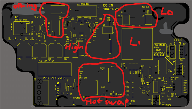
I have designed a new PCB which includes hot swap circuit, boost converter (with controller LM5122) and OR-ing circuit. Could you please review my design and provide me some suggestion?

Here are some information of the PCB:
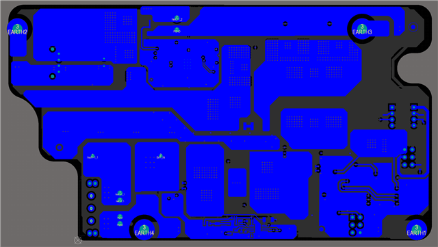
  • 4 layer board
  • 2 OZ

Please allow me to explain some key points of this new PCB layout:

  1. Power flow/high current runs on both the top and bottom layers.

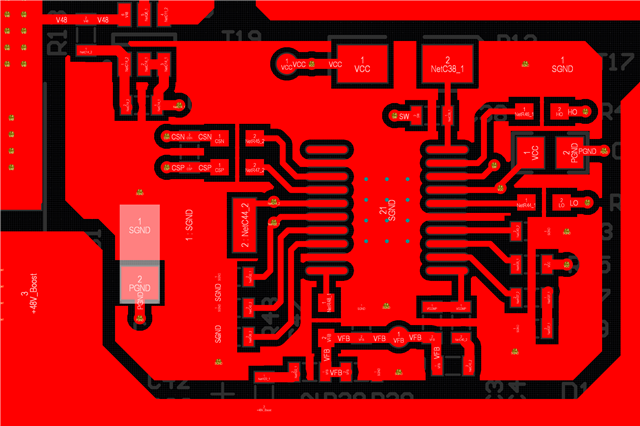
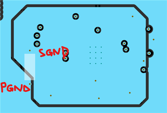
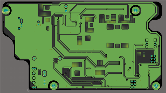
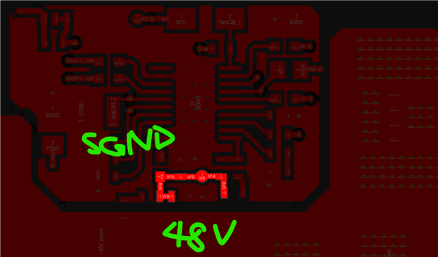
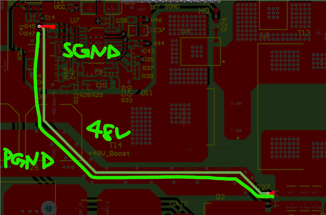
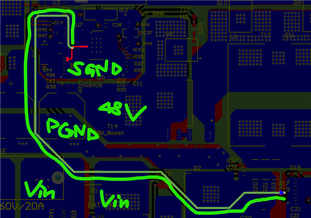
  1. Some signal traces run on the inner signal layer, while the remaining pieces on the inner signal layer are SGND (signal ground of boost) and PGND (power ground).

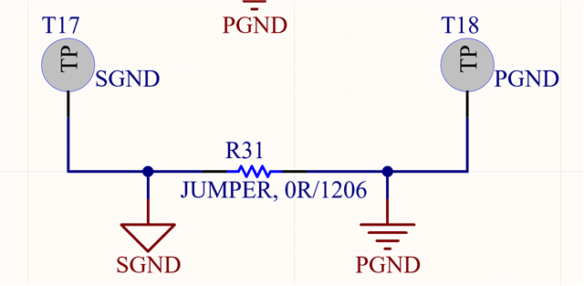
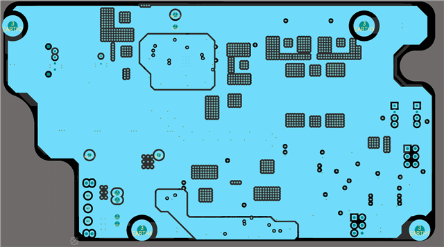
  1. The inner GND layer includes three different grounds: PGND, SGND, and LM_GND (hot swap GND). PGND is large and clear.

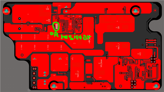
  1. The noise source is the SW node, which is the drain of the low-side MOSFET. It is also the hottest area. I have balanced the size of this area to dissipate heat adequately without emitting noise. Please see the highlighted area in the picture below: 

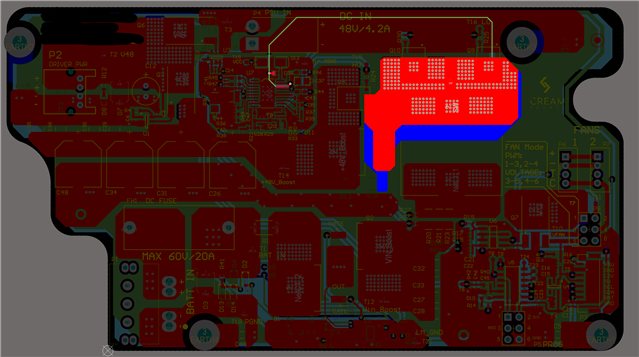
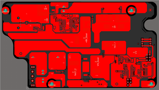
The boost controller needs to sense this voltage as a reference for the high-side MOSFET. Therefore, there is a trace from this area to the IC. However, this trace does not overlap with the control signal (highlighted in RED) and is placed as far away from the control signal as possible. It also runs on the PGND copper.

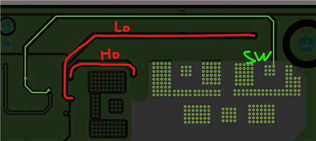
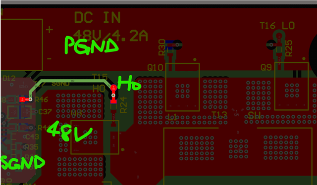
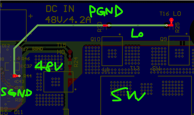
  1. Low-side and high-side MOSFET control signals run on the PGND copper (top, bottom, and inner GND layers) and are placed away from the stable 48V and SW.

  1. The output voltage feedback signal is very short and runs on the SGND copper.

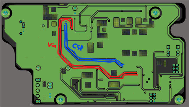
  1. Input current sensing signals (CSP, CSN) run on the PGND copper and stable 48V copper.

 .

  1. Input voltage sensing signals run on the stable DC input voltage coppers, PGND copper, and stable 48V copper.

  1. The input voltage sensing signal (highlighted in RED) and current sensing signal (highlighted in BLUE) are placed as far away from each other as possible, and their routes avoid the noise area.

  1. All MOSFETs and inductor have many vias (NOT tented) on the pads. Moreover, there are many vias (tented) used to conduct heat to the bottom next to the MOSFETs and inductor.

  1. A 48V trace flows from output at left-top corner to the header at the right hand side.

Any suggestions are opinions are appreciated. Thank you very much.

  • Hi Sean,

    Thanks for using the e2e forum.
    I can make a review of the layout and get back to you with feedback within 1-2 days.
    Can you also give me the input voltage range and the current ratings of this application? The boards says 4.2A, is this the max load?

    Thanks and best regards,
    Niklas

  • Hi Niklas,

    Thanks for your help. The detailed specification are below:

    1. Input voltage range: 12-55V (bypass mode if Vin>48V)
    2. Output: 48V / 3.75A
    3. Rated power: 180W
    4. Switching frequency: 350kHz

    Please let me know if any information are required. Thank you.

  • Hi Sean,

    Thanks again for the detailed explanations.

    I fully agree with all the changes from the previous board.
    The SW should be a better trade off in regard of thermal dissipation and noise reduction.
    The sensing lines are well placed, too.

    One open question from my side:
    Are all the inductor and FET components placed on the top side, or on the bottom? Or are some placed on top layer and some of the bottom layer?

    Thanks and best regards,
    Niklas

  • Hi Niklas,

    Thanks for your reviewing. 

    Please accept my apologies for not providing the component view. Almost all components are on the top side, especially all hot components including all MOSFETs and the inductor.

    The reason I placed all components in this manner is because I am hoping to conduct heat from the top side to the bottom side using thermal vias. Then, heat can be conducted to the aluminum plate by placing a large piece of thermal pads between the bottom side and an aluminum plate, as shown below. Do you think this approach is effective?  

  • Hi Niklas,

    I am sorry that I have one more question regarding single connection between PGND (power GND)and SGND (signal GND).

    In order to separate PGND and SGND clearly, I use a 0R/1206 resistor to connect PGND and SGND as shown below:

    It is placed on the top side (the resistor is highlighted):

    The resistor connects to PGND on the other layers using the via:

    My concern is the resistor location. It is almost located at middle of the board as shown below. Is this location ok?

    Any opinions and suggestions are appreciated. 

  • Hi Sean,

    Thanks for the update and clarification.
    Placing all power stage components on the same top layer is the best approach, so this is good.

    Regarding the AGND and PGND connection:
    The connection of both ground planes is to make sure there is no shift between the two levels. The location where the two planes connection is therefore not very important.
    Common designs use a net-tie, which is a small connections trace behaving like a 0 Ohm resistor, just without having to place a physical component. A net-tie also keeps the two plane names of AGND and PGND, so layouting is easier.
    I would recommend this approach to avoid any resistances of solder.

    Best regards,
    Niklas

  • Hi Niklas,

    Thanks for your reply and suggestion. It's very helpful!

    May I ask two more question regarding PCB layout?

    1) if there is a fan with speed control in the system, does it require an independent / isolated GND? In my case, can the fan connect to PGND as well?

    2) Regarding high side MOSFET control signal, TI provides many controller ICs integrated with internal gate drivers. Most of them, the pin of the high side control signal (HO) is between the VCC pin and the high side ground pin (HS, or SW, connected to the source pin of the high side MOSFET). I watched a TI video, and the link is below:

    Layout tips for GaN drivers

    One slide shows a good and bad example as shown below:


    My question is, is it good to place high side signal (HO) trace between a small capacitor? It means the HO signal is between VDD and HS (HS is a noise source).

    Thank you.

  • Hi Sean,

    Thanks for the feedback.

    1) There should be no problems with connecting several applications to the same GND over the board.
    As long as the other application does not inject noise into the analog ground of LM5122, I see no concerns here.

    2) It is definitely possible to route the HO signal between a cap like this. Both VDD and HO are control signals and no sensing signals, so the noise injection into each other has lower priority.
    Here it is more important to keep the HO and HS lines as close together as possible.

    Best regards,
    Niklas

  • Hi Niklas,

    Thank you for your reply. I don't have any more questions at the moment.

    I have sent my design to the PCB manufacturer. I hope it works well this time!

    I truly appreciate your assistance throughout this process. Please feel free to close this thread if it's the final step of the SOP.