Other Parts Discussed in Thread: TPSI3050, TPSI3052, TPSI3052-Q1,
A Solid-State Relay is an electronic device that acts a power switch across a barrier that provides electrical isolation. These devices have no mechanical parts and are implemented by a semiconductor, which enables higher reliability and allows for switching at higher speeds.
TPSI3050 and TPSI3052 are fully integrated isolation switch driver which when combined with an external power switch, forms a complete isolated Solid-State Relay (SSR). These are used in systems with high voltage isolation such as battery management system (BMS), factory automation and control: AC or DC output modules and more.
Both devices have a 1.5A peak source current and 3A sink current. The TPSI3052 gate driver offers voltage at 15V and the TPSI3050 has a 10V gate drive.
TPSI3050 and TPSI3052 both generate their own secondary bias supply from the power received from its primary side, so no isolated secondary supply bias is required. They have high reliability reinforced isolation, as well as lower power consumption and wider temperature ranges than traditional mechanical relays and optocouplers.
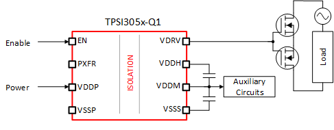
Figure 1. Basic application of TPSI305x-Q1
Setting up TPSI305x-Q1
The TPSI3050-Q1 and TPSI3052-Q1 are isolated switch drivers, providing an isolation barrier between the primary side, or control side, and the secondary side, or driving side. Both sides require supporting circuitry that varies based on need. These devices can drive MOSFETs, IGBTs, and SCRs.
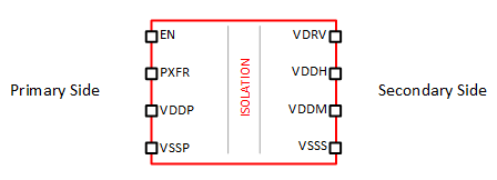
Figure 2. Pinout for TPSI3050-Q1 and TPSI3052-Q1
The distinction between the two sides is key in understanding device set-up. The connections and choices of passive components will change on each side for a different reason. Generally speaking, the set-up of the primary side is governed mainly by the choice of two-wire or three-wire mode. Conversely, the secondary side set-up changes depending on the choice of device, TPSI3050-Q1 or TPSI3052-Q1. Naturally, there are some other factors outside the choice of device and wire mode that influence device set-up, but these are simpler to understand once the high-level decision tree of figure 3 is understood.
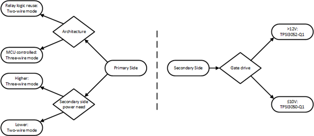
Figure 3. Set-up decision tree
Primary Side Set-up
The driving factor in setting up on the primary side is the choice of mode: two-wire or three-wire. Upon start up, the device internally detects the input voltage at the enable pin. If this voltage is above 6 V, it will self-configure internally for two-wire mode. If the voltage is below 6 V, however, it will configure to operate in three-wire mode. The device will remain in that mode until it is reset.
Two-wire Mode
Two-wire mode allows the device to reuse the logic of the mechanical relays it replaces, where two wires, one for each end of the coil, are accounted for in a design. In this set-up, a 6.5V to 48V power supply is connected to the EN pin with the primary side ground connected to the VSSP pin. Additionally, a 220nF capacitor is recommended for the VDDP pin and a 7.32kΩ-20kΩ resistor for the PXFR pin. The resistor sizing determines the amount of power transmitted across the isolation barrier where 7.32kΩ transmits the lowest and 20kΩ the highest.
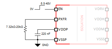
Figure 4. Two-wire mode set-up
Three-wire Mode
Three-wire mode allows the device to be implemented in a typical circuit environment, where signals are between 3V and 5.5V. In this mode, the three wires are the connections on EN, VDDP, and VSSP. Three-wire mode is capable of transmitting more power across the barrier. To set up the device for three-wire mode, a 3V to 5.5V power supply must be connected to VDDP in parallel with an 1100nF capacitance, with the primary side grounded at VSSP. A 7.32kΩ-20kΩ resistor is connected to the PXFR pin and a 3V to 5.5V signal on the EN pin turns the secondary side driver on.
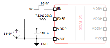
Figure 5. Three-wire mode set-up
Resistor Selection
The TPSI305x-Q1 selects the power transfer digitally based on the strength of the pulldown, thus there are specific resistance values best suited for use and are tabulated below.
|
Recommended resistors |
Two-wire mode |
Three-wire mode |
|
RPXFR, kΩ |
POUT, mW |
POUT, mW |
|
7.32 |
2.2 |
6.4 |
|
9.09 |
3.3 |
10.7 |
|
11 |
6.0 |
28.8 |
|
12.7 |
7.4 |
38.9 |
|
14.7 |
8.5 |
49.0 |
|
16.5 |
10.6 |
63.3 |
|
20 |
11.8 |
74.1 |
Secondary Side Set-up
The main difference between the two devices on the secondary side is the ratio of capacitance values between the pins and the driving voltage it creates. The internal transformer of both devices creates 5 V at the VDDM pin on the secondary side and uses a charge pump to step up the voltage for the VDDH pin, which also powers the VDRV pin. The purpose of the capacitors is to stabilize the voltages and this is most important at the VDDM pin. Since the step up is higher for TPSI3052-Q1, a larger ratio is needed to stabilize VDDM at 5 V, making the scaling between the capacitors non-linear.
TPSI3050-Q1
TPSI3050-Q1 gives a gate driving voltage of 10V at the VDRV pin, which is supplied internally from the VDDH pin. This voltage is created through the power transfer functionality of the device and stored in the capacitors CDIV1 and CDIV2, which are connected externally. In order to provide power to auxiliary circuitry, VDDM prepares 5V. To prepare 10V at VDDH and 5V at VDDM, the capacitances must follow a ratio of at least 1:1, more specifically CDIV2 ≥ CDIV1. Additional resistances are optional at the VDRV pin to limit ringing, reduce EMI, or fine-tune the gate drive strength.
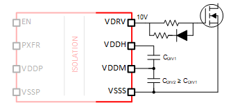
Figure 6. TPSI3050-Q1 secondary side
TPSI3052-Q1
TPSI3052-Q1 is capable of driving at 15V which means the VDDH pin will also power up to 15V. The VDDM pin will still need to charge to 5V however, so the capacitor ratio for this device must change. To achieve this voltage scheme, the ratio of CDIV2 to CDIV1 must be at least 3:1, or in other words: CDIV2 ≥ 3 × CDIV1. Like TPSI3050-Q1, additional resistance can be added to the VDRV pin to limit ringing, EMI, or fine-tune.
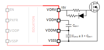
Figure 7. TPSI3052-Q1 secondary side
Capacitance Values
The next step in setting up a TPSI305x-Q1 is determining the actual capacitance values that are needed now that the ratios are understood. The best way to find these is by using the TPSI305x-Q1 design calculator linked here and also available for download on the product page of both devices. In the design calculator, select the appropriate values for a specific design in rows 6 through 14 on the user input page as shown below.
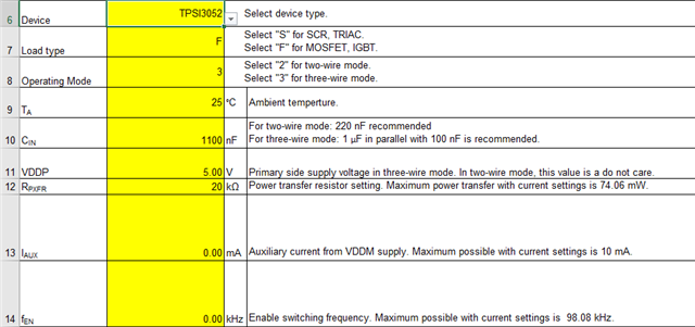
Figure 8. First rows of the design calculator
The next item needed is the charge that raises the gate voltage on the transistor from 0 V to 15 V. This can be found in the gate charge characteristics chart of a FET datasheet. Subtract the amount of charge at 0 V from that at 15 V, and enter this value into the yellow field of row 51. The gate charge characteristics chart of a FET typically looks like the figure below.
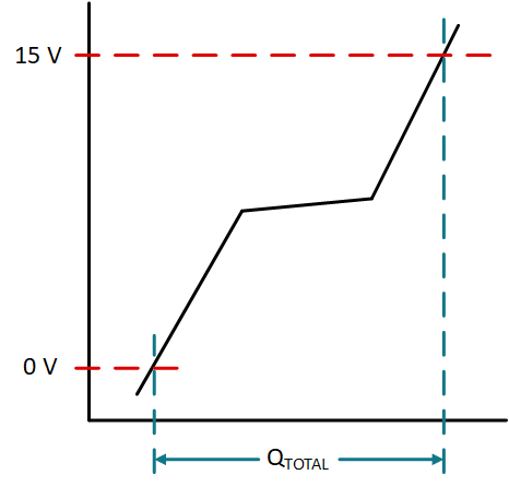
Figure 9. Gate charge characteristics
Select option B in row 52, set VDDHDROOP to 0.5 V, and enter the desired capacitance ratio to either 1.0 for TPSI3050-Q1 or 3.0 for TPSI3052-Q1. This tool will produce the minimum capacitances necessary to drive the FET(s) in rows 67 and 68.
The droop on VDDH is the amount the voltage dips when VDRV is enabled. It is important that this value is limited to 0.5 V since too great a droop will trigger undervoltage lockout on the VDDH pin, de-asserting the VDRV pin.
FET Driving Capabilities of TPSI305x-Q1
TPSI305x-Q1 can support a wide variety of FET sizes and switching speeds of up to 100 kHz. The power transfer functionality of the device delivers a finite pool of power. To determine the resistor sizing needed for a given switching speed, refer to the design calculator and populate the fields up to and including the QTOTAL of the transistors. Larger transistors require more gate charge and thus switch slower, making this and the power transfer resistance the limiting factors of the switching speed.
Powering Auxiliary Circuits from VDDM
TPSI305x-Q1 also brings value in its ability to power auxiliary circuits from the VDDM pin. In a static switching solution, up to 50 mW of power is available. This can be used for current or temperature sensing circuits as an example. In non-static solutions, the power becomes more of a shared resource between the FET switching circuits and auxiliary circuits. The easiest way to determine the power available to auxiliary circuits is to refer to the design calculator tool.
Gate Driver Output Resistance (RGSRC and RGSNK)
Optional resistances can be added to the gate of the device being driven for a couple reasons. They can help to limit ringing from switching, reduce EMI, or help to fine-tune the drive strength. RGSRC can limit the source current from the internal pullup structure to a value less than 1.5A. Similarly, RGSNK limits the current from the internal pulldown structure to a value less than 3A. It is important to note that the sink and source currents are not constant, but pulse-like functions that decay over time like a discharging capacitor.
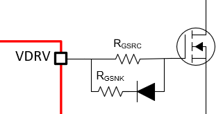
Figure 10. Gate resistances at VDRV output
A pulldown can also be added from the gate to the source of the transistor to keep the gate low when the device is not in operation. It is important to note that this method siphons power from the driver when the device is enabled, leading to a slower turn-on.
Examples of Applications
The TPSI305x-Q1 family can be used in a wide variety of applications. Despite this, the decision hierarchy remains relatively simple for the designer. For the decision between two and three wire mode, it is a question of control logic and power need. For the decision between TPSI3050-Q1 and TPSI3052-Q1, it is a decision between the gate drive needed.
Outlined below are the design requirements for an application that needs an isolated switch driver:
|
Load type |
AC |
|
Switching |
Dynamic, >50kHz |
|
Gate drive |
>12 V |
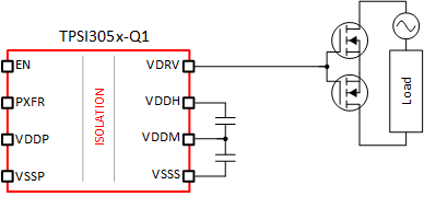
Figure 11. TPSI305x driving back to back FETs
Based on these design requirements, it is apparent that the FETs will require considerable power to drive for two reasons in particular. First, it is an AC load and so two FETs are required to provide blocking in both directions. Second, it will be switching at a frequency that is towards the upper limits of the device’s capability. The higher switching frequencies require constant replenishment of charge in the secondary side capacitors and thus that the power transfer system is active more frequently. This higher power transfer need requires a three-wire mode configuration. Switching of this kind may imply that a microcontroller is controlling the isolated driver. Three-wire mode is better suited for microcontroller use. The gate drive requirement of at least 12 V means that the device most apt for this application is the TPSI3052-Q1.
Consider the design requirements of a second application:
|
Load type |
DC |
|
Switching |
Static |
|
Gate drive |
10 V |
From these requirements, it is very clear that the power requirement for this application is much lower due to the fact that it is a static switching, DC (single FET) application. This is a scenario that two-wire mode could be suited for. The two-wire mode functionality of the TPSI305x-Q1 devices enables drop in replacement of mechanical relays, its name connotates the two terminals of a coil. With the 10 V gate drive of this design, the best device is the TPSI3050-Q1.
Conclusion
When paired with an external switch the TPSI305x-Q1 devices create a seamless solid-state relay. Due to the wide variety of possible uses for this device, the application circuit varies. Despite this, the circuits for both the primary and secondary side can be understood easily. For the primary side, the consideration is the power and architecture: discrete relay replacement or MCU driven. On the secondary side, a designer will choose between the two devices based on the gate drive needed. With these concepts in mind, designing the TPSI305x-Q1 into an application will be more straightforward.

