


Other Parts Discussed in Thread: TPSI3100-Q1, TPSI3052-Q1
As MOSFETs are used across so many industries and applications, the shear breadth of options and vendors is seemingly endless. In the same vein, the range of factors that play a part in determining a MOSFETs suitability for a particular application can seem nebulous. This FAQ will answer the question in a digestible way, going over the most important of the factors to consider when selecting a MOSFET to pair with the TPSI305x-Q1 devices and the TPSI3100-Q1 using a common application as an example.
System Introduction
In an electric vehicle, the high voltage rail coming from the battery is stabilized by a capacitor known as the DC-Link capacitor. This capacitor limits fluctuations in the rail as systems draw current sporadically, such as a traction inverter. A pre-charge switch charges the capacitor on startup and a switch connected to the negative rail discharges the capacitor when the vehicle is parked and turned off. For this example, the battery voltage is 400 V and the resistors in series with the FETs are 50 Ω.
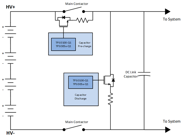
Figure 1. Isolated switch drivers in an EV battery management system
The first considerations for our MOSFET come from the system it is designed in to. The next considerations will concern the current, power, and thermal resistance of the FET.
System Requirements (MOSFET Inputs)
System Voltage – As outlined, the system voltage is 400 V. This voltage determines the breakdown voltage of the FET. However, a FET with 400 V breakdown is not suitable because any variation in the voltage above that rating could cause damage to the FET. Another factor to consider is that an EV battery’s full charge may reach voltages of 500 V. It is best practice to give a margin of at least 20% above the maximum expected voltage. In this case, the rated breakdown voltage the FET needs is 600 V.
Gate voltage – The second system input to the FET to keep in mind is the gate-to-source voltage, or the voltage that will turn on the FET. A 15V drive voltage is provided by TPSI3100-Q1 and TPSI3052-Q1. As the selection is narrowed down, it is important to confirm the on-resistance at a 15 V gate-source voltage. The on-resistance varies with junction temperature as well, however many datasheets will include on-resistance as a function of junction temperature or gate-source voltage. For the purposes of this FAQ, the maximum on-resistance will be used.
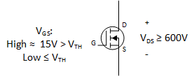
Figure 2. MOSFET system inputs
Based on the system inputs discussed thus far, the three candidates below are suitable. Each of them has a VDS of at least 600 V and report different on-resistances at the maximum junction temperature and a VGS of 15 V.
MOSFET A:
- VDS = 650 V, ID = 46 A
- RDSON = 70 mΩ
- RthJ-mb = 0.88 °C/W
MOSFET B:
- VDS = 650 V, ID = 21 A
- RDSON = 156 mΩ
- RthJ-mb = 1.17 °C/W
MOSFET C:
- VDS = 650 V, ID = 19 A
- RDSON = 346 mΩ
- RthJ-mb = 2.3 °C/W
Current and Power Considerations
The next step is to determine if the current and VDS it creates lies in the safe operating area (SOA) of each FET. When the FET turns on, the current flowing through is expected to peak at 8 A, however this could go as high as 10 A. On the MOSFET datasheet, there is generally a safe operating curve that charts drain current as a function of the drain-source voltage. As a starting point that requires no calculations, it is good to check that the expected current falls below the pulse current maximum with some margin. For this FAQ, 50% margin will be used since the pulse is longer that 100 ms and the FET must withstand it without any additional heatsinking. This does not mean half of the current itself since the charts are scaled logarithmically. If there is not enough margin, the FET is likely not suitable.
To confirm more precisely the suitability of each FET, an estimate of the power dissipation limit can be calculated. This equation is similar to the equation for deriving the junction-to-ambient thermal resistance:
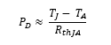
The equation used here will replace the junction-to-ambient thermal resistance (RthJA) with the junction-to-mounting bracket thermal resistance (RthJ-mb). The equation can also be arranged to calculate VDS after substituting the product of drain current and drain-to-source voltage for power. The temperature at the junction will be considered to be at its maximum since that is the limiting factor of the material and the temperature at the mounting bracket will be 25 °C.
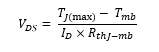
This equation was used to calculate the drain-to-source voltages of each of the candidate devices with a drain current of 10 A.
- VDS = 17 V
- VDS = 12.8 V
- VDS = 6.52 V
Now that the voltage values are calculated, refer to the SOA chart to confirm that the device is suitable. Below is an example of a typical SOA curve with the RDSon curve on the left, the current limit at the top, and the power limit curves on the right. Ensure that the intersection of the 10 A line and calculated VDS are below the lowest power limit curve and below the RDSon curve on the left. Be sure to use the SOA curve in the device datasheet, not the one in this FAQ as it is only an example. For the devices discussed in this FAQ, A and B make this condition, however device C cannot. This shows that despite its drain current rating of 19 A, it cannot actually be used in this design.
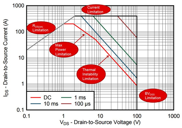
Figure 3. Example of MOSFET SOA curve
It is also important to reiterate the need of margin. Although the calculation is more exact, it is best to give some margin on top of it. Although this can mean higher costs, it also makes the design safer.
Additional Considerations for Other Applications
In the example considered above, power dissipation was not constrained, as in there was no limit to how much power the transistor was allowed to dissipate. As this is not a likely scenario, this section will cover some common sources of power loss in MOSFETs.
Power
Often times, designers will set out to maximize power efficiency by minimizing losses. Three sources of power loss in a FET come from heat dissipated from the current flowing through the FET and the power dissipated in turning the FET on. They are known as conduction and switching losses, respectively.
- Conduction losses – As discussed earlier, power dissipation is at its lowest for a particular FET when it is conducting at its lowest on-resistance. Although this resistance varies with thermal fluctuation, selecting a gate-to-source voltage that can achieve this on-resistance is desirable.
- Switching losses – A FET dissipates additional power during the transition between on and off. This loss is insignificant in static switching since the time spent in the transitory stage is so small. However, in switching applications, this power dissipation becomes non-negligible.
- Gate losses – To turn a FET on and off, the gate capacitance must be charged and discharged. Similar to switching losses, this plays its biggest role in switching applications. These losses can be minimized by selecting FETs with short turn on and turn off delays.
Heat Dissipation
In high power circuits, heat dissipation is an important aspect of the design as it creates destructive, positive feedback loop if left unchecked. If a design with a FET that must conduct a linear, constant drain current, a possible solution is to attach a heatsink to the FET and scrutinize the layout of the design more closely. By attaching a heatsink, the value of the junction-to-ambient thermal resistance reduced and can perhaps enable the use of a smaller, more cost-efficient FET. Additionally, small layout changes that afford the FET more are can help to make the heatsinking more efficient.
Conclusion
Finding the FET that works best with TPSI310x and TPSI305x for a specific application can seem like a difficult task since there are so many FET characteristics to consider and many vendors to choose from. Luckily, the decision can be made a lot simpler by looking at the system inputs to the FET, and then making some simple calculations for current, power, and referring to the safe operating area curves.
To learn more about TPSI305x and TPSI310x, visit their product pages on here.
