This thread has been locked.

If you have a related question, please click the "Ask a related question" button in the top right corner. The newly created question will be automatically linked to this question.

UC3525A: UC3525A waveforms issue

Part Number: UC3525A

Hi Team,

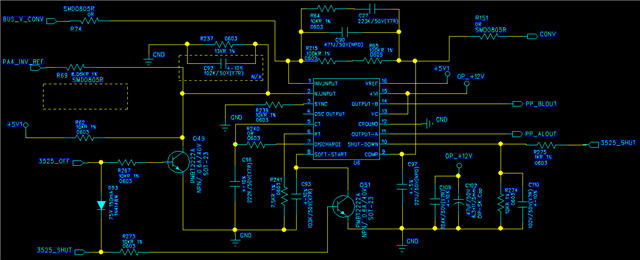
Please refer to the schematic, 

Customers use UC3525 to create push-pull topology;
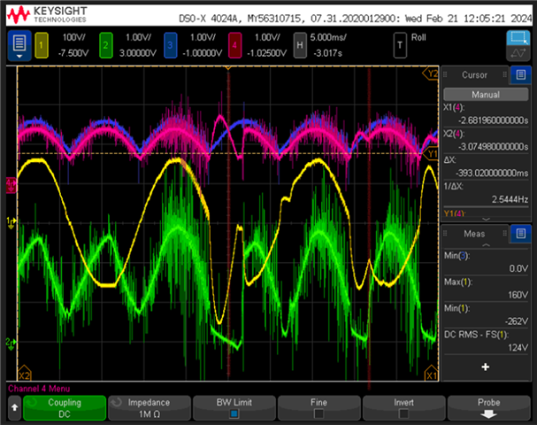
CH1: Vo (yellow)
CH2: COMP (pin 9/green)
CH3: OP+ terminal (pin 2/blue)
CH4: OP - terminal (pin 1/red)

Under normal circumstances, pin4 will follow the pin3 waveform (pin4 is higher than pin3, comp low level, duty off; pin4 is lower than pin3, comp high level, duty).

However, in the middle of the reference waveform, pin4 is lower than pin3, and comp still maintains the low level for about 1 ms before turning to the high level.

Under normal circumstances, COMP will immediately reflect the difference between the two ends of the OP.
However, when a specific load is instantaneously switched (such as waveform), COMP will reflect the delay.
What could cause this phenomenon?

  • Rock,

    Can you show a Bode plot of the compensated control loop? This will give an indication of how the control loop ought to be performing. I'm not sure why R215+R65 is in the circuit? Also, why C97 is in the circuit? From the scope plot you attached, the COMP signal appears to have much high frequency noise and this could be GND noise picked up from C97 or something else in the PCB coupling noise into the COMP signal. The more typical Type 3 compensator we see used for VMC would look like figure 4 here. Also, once the Bode plot is determined, please be aware of the GBW limits of the UC3525 op amp which are given in figure 4 here.

    Regards,

    Steve