This thread has been locked.

If you have a related question, please click the "Ask a related question" button in the top right corner. The newly created question will be automatically linked to this question.

TPS65220: Request a TPS65220 circuit review and related inquiries Request a review

Part Number: TPS65220
Other Parts Discussed in Thread: TPS6521905

Hi, TI expert

A customer has a question while reviewing TPS65220.

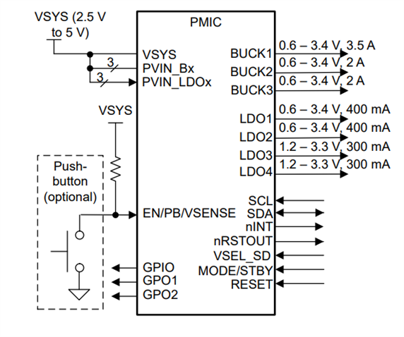
Q1) The attached file is a TPS65220(PMIC) block circuit diagram, and we would like to request a circuit review before PCB Artwork.

7450.PMIC.pdf

Q2) The information below is what the F/W manager inquired about. Please review the contents.

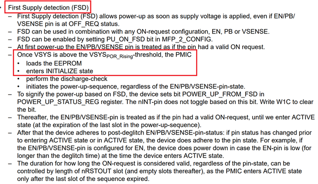
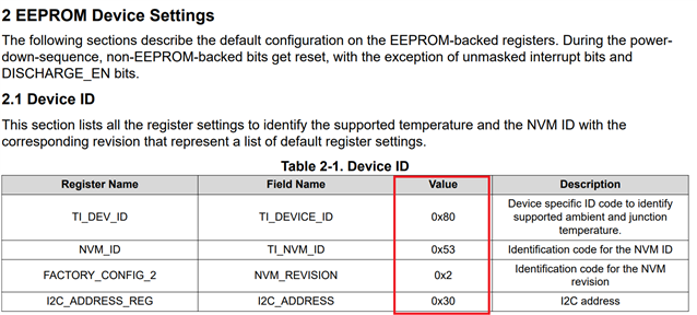
- I'm curious if the default values in the TPS6522053 Technical Reference Manual are correct for the PMIC. Initially, when power is supplied to the PMIC as shown below, it always enters FSD (First Supply Detection) Initialize mode and retrieves EEPROM values. Could you confirm if the default values mentioned in the manual are accurate?
Please check. Thank you.

  • Hi,

    Thank You for using E2E. What processor/SoC or application are you powering with the TPS65220 PMIC? The settings in the schematic seem custom and might not match the default configuration on TPS6522053. For custom NVM configurations we recommend using the user-programable version (TPS6521905). Here is the link to the programming guide: https://www.ti.com/lit/pdf/slvucm5.

    • First supply detection (FSD) is enabled by default, This means the PMIC ignores the state of the EN/PB/VSENSE pin and executes the power-up sequence as soon as VSYS goes above the POR threshold. FSD is only applicable during the first power-up (until nRSTOUT is released). 

    • The notes about the EN/PB/VSENSE pin are not correct. This pin is configured as "Enable" instead of "Push-button" in the TPS6522053 NVM. This information is included in the TRM. 

    • TPS6522053 has the Bucks configure to operate in Quasi-Fixed Frequency and high bandwidth. This mode requires a minimum of 30uF local output capacitance on each Buck (47uF per Buck is typically used). 

    • The maximum local output capacitance (close to the pin) on each LDO is 4uF. I recommend lowering the local capacitance on VLDO4.

    • It is recommended to use a 100k Ohms pull-up resistor on EN/PB/VSENSE. I recommend increasing R401.

    • Couldn't find the pull-up resistors for the I2C pins (SDA/SCL) but I'll assume this exist in other pages of the full schematic.

    • Just as a reminder, GPIO and GPO1 are disabled by default and can only be enabled by I2C after the PMIC finished the power-up sequence.

    • For reference: the MODE/RESET is configured as warm reset (register settings get reset to the default values after a falling edge is detected). 

    • The VSEL_SD pin is configured to set the output voltage on LDO1. A pull-down on this digital pin will set an output voltage of 1.8V on LDO1. Here is how the VSEL_SD was configured:
      • VSEL_SD HIGH, LDO1 = 3.3V (behaves as bypass, similar to load-switch and requires PVIN_LDO1 = 3.3V)
      • VSEL_SD LOW, LDO1 = 1.8V (behaves as a fixed 1.8V LDO)

    Thanks,

    Brenda

  • Hi, Brenda

    Thanks for reply.

    The application the customer is reviewing is cold chain (smart tracker).
    The block diagram is as follows, and the PMIC is being reviewed as TPS65220.

    1222.(Block Diagram).pptx

    Do you have any additional advice?

  • Hi Grady,

    The device expert is currently out of the office. When they return they will look into this and provide a response. Please expect some delay accordingly.

    Thanks,
    Field

  • Thanks for Field.

    I'll be waiting, and I have further inquiries.

    Dear, Brenda

    Customers have additional inquiries regarding H/W.

    (Brenda said)  *The notes about the EN/PB/VSENSE pin are not correct. This pin is configured as "Enable" instead of "Push-button" in the TPS6522053 NVM.

    This information is included in the TRM.

    Question 1) Referring to the contents below on the DATA-SHEET, I designed the circuit because I thought it could be used as the POWER ON/OFF KEY of the DUT by using the Push-button Option. If there is an error in this part, can you tell me what part of the circuit or F/W needs to be modified to implement the POWER ON/OFF KEY of the DUT?

    For your reference, the content below has been modified based on your response.

    1) TPS6522053 has the Bucks configure to operate in Quasi-Fixed Frequency and high bandwidth. This mode requires a minimum of 30uF local output capacitance on each Buck (47uF per Buck is typically used). 

    → BUCK 1/2/3 OUT-PUT: 47uF applied

    2) The maximum local output capacitance (close to the pin) on each LDO is 4uF. I recommend lowering the local capacitance on VLDO4.

    → R401: 100K applied

    3) Couldn't find the pull-up resistors for the I2C pins (SDA/SCL) but I'll assume this exist in other pages of the full schematic.

    → OK

    4) For reference: the MODE/RESET is configured as warm reset (register settings get reset to the default values after a falling edge is detected).

    → OK

    5) The VSEL_SD pin is configured to set the output voltage on LDO1. A pull-down on this digital pin will set an output voltage of 1.8V on LDO1. Here is how the VSEL_SD was configured:
    VSEL_SD HIGH, LDO1 = 3.3V (behaves as bypass, similar to load-switch and requires PVIN_LDO1 = 3.3V)

    → OK

    Please check. Thanks

  • Hi Grady,

    Brenda is out of office for two weeks, so I am going to re-assign this thread to someone to help you while she is out. Please expect feedback tomorrow on the question about the EN/PB/VSENSE pin.

    Best regards,

    Matt

  • Hi Grady,

    Since the EN/PB/VSENSE pin is in the Device Enable Configuration by default, you will need to reprogram the device and write R20 bits [5:4] = 01b to switch to Push Button Configuration.

    Also, if you don't want the device to power up when VSYS is first applied, you need to disable First Supply Detection (FSD) by writing R20 bit [7] = 0b.

    In Brenda's original reply she mentioned the TPS6521905 because this is the device we recommend for custom programming. We recommend this option because it helps us keep track of ICs that may have unique programming that is different from our pre-defined IC versions.

    You can change the programming of the IC version you have currently, but I would only recommend this course of action for short term testing purposes. If you need a custom program for full production I would move to the TPS6521905.

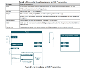
    The programming guide linked by Brenda above goes into detail about the programming process. On-board programming is possible, but it requires VSYS to be above 3.3V and you need access to the I2C lines. The SCL and SDA lines will need a 3.3V pull up and there are a few external components that are required as shown in the diagram below.

    One benefit of the TPS6521905 is that you can apply VSYS voltage without enabling any rail output voltages since the IC programming is blank to begin with.

    For the TPS6522053 version of the PMIC, the Push Button hold time required to trigger power up is 200ms by default (short deglitch). Based on your block diagram, your target is 600ms (long deglitch) so you will also need to write R20 bit [3] = 1b as part of the reprogramming process.

    R20 is the MFP_2_CONFIG Register for reference.

    Regards,

    James