Hello,
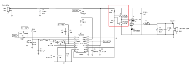
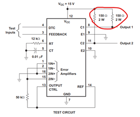
I plan to make a design with TL494. But here I could not understand the high wattage values of the resistors connected to the output pins. What is the reason for this?
Hello,
I plan to make a design with TL494. But here I could not understand the high wattage values of the resistors connected to the output pins. What is the reason for this?