This thread has been locked.

If you have a related question, please click the "Ask a related question" button in the top right corner. The newly created question will be automatically linked to this question.

LM66100: Reverse current blocking configuration losses

Part Number: LM66100

I am considering the LM66100 configuration which would provide reverse current blocking from the datasheet:
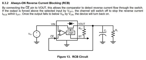
The device turns ON when VCE is approximately 250mV BELOW Vin   (VIN - VCE > 250mV)

Doesn't this mean that when using the reverse current blocking configuration, Vout will be 250mV BELOW Vin, and therefore the internal PFET is actually operating in the linear region?

If my understanding is correct, there will be additional losses when using this configuration and we will not achieve the ideal diode behavior.

  • Hi Jim,

    The LM66100's main FET uses logic and a driver to ensure it is either off or fully on at any time. It doesn't operate in the linear region, and the output of the CE/VIN comparator feeds into digital-type logic, not directly to the gate.

    Thanks,

    Patrick

  • I think I'm confused at how this configuration works in that case.

    The device is ON when VIN-VCE > 250mV approximately.

    If VCE = VOUT as shown in the schematic, then the device will be ON when VIN-VOUT > 250mV

    This means that VOUT must be below VIN.

    How is this achieved if the device is only either fully on or fully off?

  • Hi Jim,

    I apologize if I misunderstood your question.

    Consider a situation where VOUT is being driven with a voltage higher than VIN. The device will turn the FET off (VGS = 0V, Vgate = VIN) when VOUT (CE) is 80mV max higher than VIN, so current doesn't flow from VOUT to VIN or from VIN to VOUT. Then, when VOUT (CE) drops 250mV max below VIN, the device will turn the FET back ON fully (to its datasheet spec'd Ron value), and then current can flow from VIN to VOUT or VOUT to VIN. For example, if you are using a 3.3V battery on VIN and a circuit + 5V wall supply on VOUT, when the 5V wall supply is connected the device will turn the FET off to prevent reverse current, then when it is removed the FET will turn back on so the battery can power the circuit.

    The device doesn't regulate the VIN to VOUT voltage, it only turns the FET on if VIN > CE + 250mV max, and turns it off if VIN < CE - 80mV max. When CE is between the turn-on and turn-off values, the FET state depends on what the previous CE state was (like a simple comparator with hysteresis).

    Am I still misunderstanding your question?

    Thanks,

    Patrick

  • Patrick - thanks for your replies so far.

    Let's just consider the circuit above from the datasheet, no external source connected to Vout. How does this work?

    If we walk it through in time, let's say the source Vin is connected via a switch which closes at t0.
    Let's also assume the source Vin is 5.0V and that there is some input capacitance on the IC pin VIN.

    So before t0:
    Vin = 0V
    VCE = VOUT = 0V

    Now the switch closes at t0, and the voltage at the input pin VIN begins charging from 0V up.
    Table 6.3 of the datasheet says the minimum VIN voltage is 1.5V so let's assume nothing happens before that.

    So before the voltage at VIN hit's 1.5V, we have:
    0V < Vin < 1.5V
    VCE = VOUT = 0V
    Device is OFF

    Now let's move forward in time. Vin hit's 1.5V
    Vin = 1.5V
    VCE = VOUT = 0V
    Vin - VCE > 250mV so device turns ON and is conducting VIN to VOUT

    Now let's step forward one more step right after the device has turned on
    Vin > 1.5V
    VCE = VOUT = VIN = some voltage above 1.5V
    So now VOUT = VIN but VCE also equals VOUT
    Vin - VCE = 0V
    The device should now turn OFF

    How can the device remain on at all in the circuit shown above unless Vout is less than Vin?

  • Hi Jim,

    Ah, I see the confusion now. The condition for turning the device OFF is VOUT - VIN = VOFF (35mV typ, 80mV max). If VOUT - VIN has not exceeded that value, then the device will stay ON. However, if VOUT - VIN does exceed VOFF and the device turns OFF, THEN the condition needed to turn the device back ON is VOUT - VIN = Von (-150mV typ, -250mV max). In your example above, the device would still be ON because VOUT (VCE) - VIN hadn't exceeded VOFF.

    Please see the second sentence of the paragraph in the image you sent in your original post.

    Thanks,

    Patrick

  • Thank you Patrick, I understand now. Much appreciated.