This thread has been locked.

If you have a related question, please click the "Ask a related question" button in the top right corner. The newly created question will be automatically linked to this question.

TPS55289: Schematic Check

Part Number: TPS55289

Could someone please check my schematic for the TPS55289? I want to output variable voltage (0.8V-21V) with up to 2A load current.

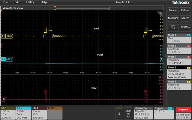
With the current schematic, I am able to output voltages <5V quite accurately albeit with some ripple.

Attached below are some test results.

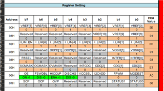
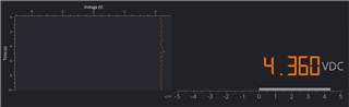
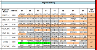
Figure-1 contains the register settings I have used to obtain 4.3V output voltage using 9V Input Voltage. Figure-2 contains the waveform of the output ripple (varies between 4.25 and 4.5V. Not great but I can live with it).

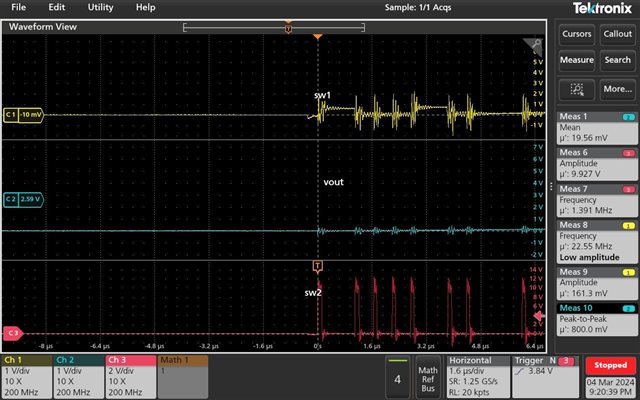
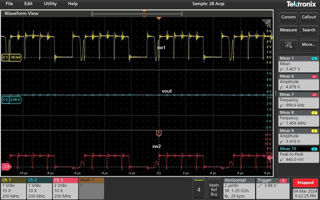
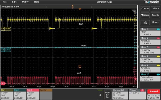
My problem right now is to obtain values greater than 5V.

If I configure the TPS55289 to give Vout= 12V with Vin=9V using the following register settings:

I get the following output voltage waveform

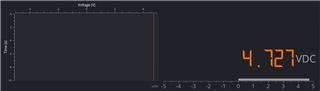
It is either stabilizing at a random voltage (4.727V when I ran the test for writing this post) or jumps to 5.1V and then the voltage very slowly decays to 0.1V.

Is this a loop stability issue or is there something wrong with my schematic?

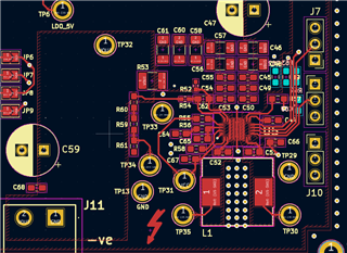
Inductor Part Number: SPM10065VT-4R7M-D (4.7uH)
Capacitor Part Number: CL31B106KAHNFNE (10uF Ceramic Cap)

I am also attaching a .pdf version of the schematic for reference below

USBC_Power_Supply-Output_Channel_1-TPS55289.pdf

  • Hi Krishna,

    Thanks for reaching out. 

    What is the parr number of the output capacitor C59?

    Can you share the waveforms of SW1, SW2, Vout and inductor current?

    BRs,

    Bryce

  • I have used a generic 100uF_25V Aluminum Electrolytic Capacitor that is sourced locally here. Can't get information regarding its part number and ESR value.

    Scenario-1

    Vin = 5.2V; Vout = 1V; Load = 22 Ohms

    Waveform for Scenario-1:

    Scenario-2

    Vin = 10V; Vout = 7V; Load = 22 Ohms

    Waveform for Scenario-2

    Scenario-3

    Vin = 5V; Vout = 7V; Load = 22 Ohms

    Waveform for Scenario-3

    Scenario-4

    Vin = 5V; Vout = 3.3V; Load = 22 Ohms

    Waveform for Scenario-4

    I couldn't get the inductor current waveforms as I don't access to a current probe currently.

    Additional symptoms noticed while debugging today:

    1) The converter stops switching when the input voltage rises above 7.2V which seems to be a deviation from the OVP Threshold mentioned in the datasheet (23.5V). This was observed when we increased the input voltage slowly using a power supply

    2) The STATUS Register always responds with 0x00 even when the converter is operating in Buck Mode. According to the datasheet, Buck Mode Nominal operation should return 0x01.

    3) Converter switches to Boost Operation when the requested output voltage is set to be below 5V. But even when output voltage >5V is requested, the voltage either clips to ~5.1V or the converter stops switching and the output voltage slowly decays (Vout discharge is disabled).

  • Hi Krishna,

    Sorry for late reply, from the register value and the waveforms, the device operates at PFM mode, thus the voltage ripple you mentioned at 4.3Vout is large, you can change the mode to FPWM to obtain smaller voltage ripple.

    And from the waveforms from scenior1 to scenior3, it doesn't make sense the high voltage level of SW1 doesn't equal to Vin and high voltage level of SW2 doesn't equal to Vout. Can you also check if the input voltage equals to the value you set? And what is the input power supply current limit value?

    BRs,

    Bryce

  • Hello,

    Sorry for getting back to this so late.

    I've double checked the input power supply, it remains stable at 9V.
    The source is a bench-top power supply set with a current limit of around 10A. It doesn't seem to be a input power rail issue.

    Any help here would be appreciated. I plan to open-source the design anyway. Let me know if you need anymore information regarding the board.

    Regards,

    Swaroop

  • Hi Krishna,

    1. Can you also share the layout of TPS55289 here?

    2. And can you probe Vin, SW1, SW2 and Vout waveforms at the same page?

    3. Does this phenomena happen at all boards or just one board? Can you try on another board with one new silicon to prevent the soldering issue?

    BRs,

    Bryce

  • Please find the Layout for TPS55289 below:

    KiCAD ScreenShot:

    Top Layer:

    Bottom Layer:

    2) Will get back to you with these waveforms in a while.

    3) This was meant to be a prototype run to evaluate the output performance of the IC. I will try using another IC and get back to you.

  • Hi Krishna,

    Thanks for your feedback.

    The layout is not good especially for the relief connection of GND connection which would introduce a lot parasitic parameters into power loop.

    Looking forward to your further feedbacks.

    BRs,

    Bryce

  • Hi Krishna,

    We have not seen an update from you for four weeks, so I assume the questions are answered and the issue is solved.

    I close this thread now. If there is still something open, please reply and the thread will get opened again.

    If you have any other question or of the thread has been locked, please open a new one.

    Best regards,

    Bryce