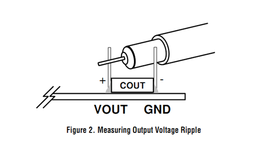
This thread has been locked.

If you have a related question, please click the "Ask a related question" button in the top right corner. The newly created question will be automatically linked to this question.

Switching Noise on TPS61087 Output

Other Parts Discussed in Thread: TPS61087

Hi,

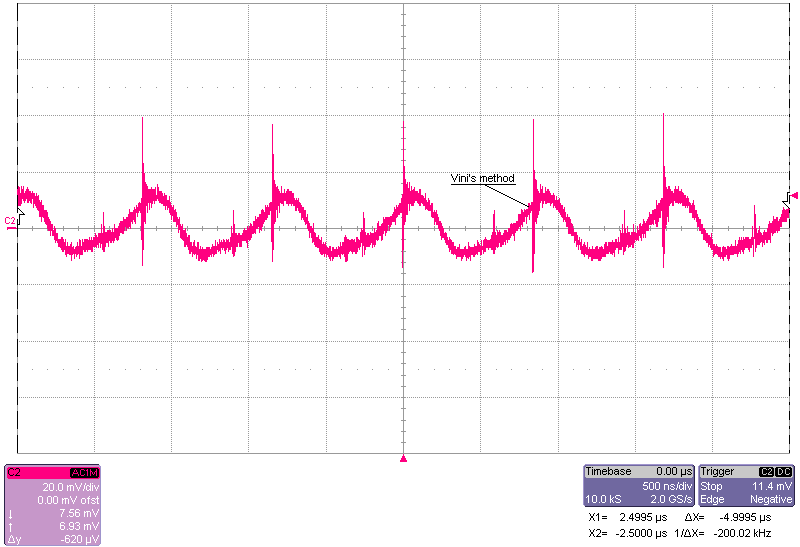
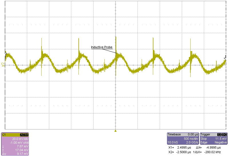
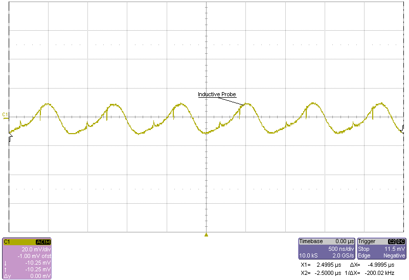
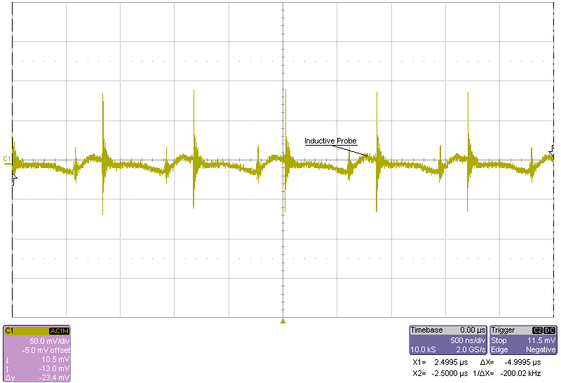
I am using TPS61087 for generating 7.5V from 5V. I am seeing a high frequency noise on the output as shown in the image given below


Here are the design parameters

  1. The 7.5V output is used to drive a motor which can draw from a min of 50mA to a max of 500mA current. So design is done for 500mA load.
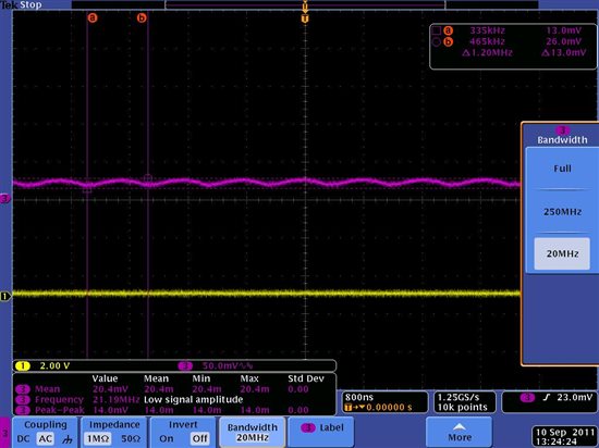
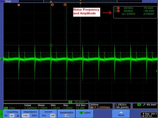
  2. Switching frequency is selected as 1.2MHz .
  3. Input cap is 10uF in parallel to 1uF.
  4. Output caps are two 22uF/25V in parallel.
  5. Inductor is 10uH with a saturation current of 1.9A
  6. An RC is used at COMP pin for compensation (R=100K, C=1nF)

The waveform shown above is captured with a DC resistive load of ~275mA. 

Can anyone tell me if I am missing anything here?

I think this kind of switching noise is inherent to switching DC/DC converters but amplitude a more here and that too with a uniform load. Has anyone else seen this issue with TPS61087?

Vini


  • How are you measuring the ripple?  You need to use a low inductance probe to not pick up switching noise that is not really there.  Take the 'hat' off the probe tip, put a wire wrap around the probe barrel for the ground connection, and look at Vout right across the output cap.

  • Hi Chris,

    I am measuring the ripple right across the output cap as shown below and still seeing the noise.

    I was just doubting my compensation network. As the load range is 100mA - 500mA and value of compensation components depends on load, so, I am not sure which values to put actually. I tried some different values and as per SwitchPro, the gain and phase margins are sufficient for these values, but still noise is there.

    Vini

  • Vini,

    If the compensation network was causing this noise you would see a low frequency signal, and the system might not be stable.  So I don't think that is your problem.

    I think that if you modify your oscilloscope's bandwidth settings to 20MHz instead of the "Full" setting, then you will see a much nicer waveform.  The noise that you were concerned about is at 1.2MHz, which the 20MHz bandlimit should be able to display, if that was what you were seeing.  I've attached some waveforms so that you can see the difference changing this one setting makes.  This first one was measured by copying the illustration you made above and uses the "Full" bandwidth setting.  I measured across C10 on our EVM for the next three waveforms.

      This next one was done by using the low inductance probe that Chris described above and uses the "Full" bandwidth setting.  Notice that the two waveforms are nearly identical. 

    This next one uses the low inductance probe with the normal 20MHz bandlimited setting. 

    Finally, since I still wasn't seeing the magnitude of noise spikes that you were, I measured across a different output capacitor, C7 on our EVM schematic, at the full bandwidth setting again.  This more than doubled the amplitude of the spikes.  Make sure that you are measuring across the capacitor closest to the output, it does make a difference in the amount of noise you will see.  Take a look at the EVM schematic that we make for this part to see the physical location of these two caps.  The EVM's user guide can be found here.

    If this doens't fix the problem for you, could you let me see your board layout?  An improper layout can also add to the noise.

    -Clancy 


  • Hi Clancy,

    We are using two TPS61087 ICs in our design and this noise is seen on the output of both the regulators. The schematics and board layout are attached here. This is a 8-Layer board. I have shown the relevant 4 layers. There are 2 additional signal & PWR/GND layers not shown.

    4645.TPS61087_Schematics.pdf

    3660.TPS61087_Layout.pdf

    Here also when bandwidth of probe is limited to 20MHz, the high frequency spikes are filtered and not seen in oscilloscope as shown below


    Also, I probed on a cap which is on other side of PCB (far away from regulator) and actually there is no noise there even with full bandwidth setting of probe.

    One thing is sure here that there is high frequency noise, especially near the regulators (with a frequency content of more than 20MHz as oscilloscope just suppresses these frequencies when bandwidth is limited to 20MHz). Now my doubts are

    What are sources of this noise? As the spikes are repeated at a frequency equal to the switching frequency of TPS61087, it seems that this noise is due to IC.

    Or is this due to inductor? We are using shielded inductors and part numbers are given in attached schematics.

    This noise may certainly cause EMI/EMC issues. Though I have not seen this kind of noise with all the DC/DC converters I have used but I remember one example from my previous design,  where a boost converter from TI was causing radiated emissions and we were able to pass the RE test after removing that part. Is this kind of noise expected from all the boost converters?

    Vini

  • Vini,


    This is normal behavior for a boost converter.  In fact, all switching converters are going to exhibit this behavior.


    The problem is that parasitic capacitance and inductance cause ringing and current and voltage spikes whenever the FETs switch.  These parasitic components occur internal to the switching power supply (FETs have drain to source capacitance, bond wires have some inductance) and occur due to the board layout (every trace has inductance and capacitance).  Consider for example the parasitic capacitance across the diode in this design.  The voltage at the SW node is switching from approximately 0V to Vout+V_diode_drop.  Since I=Cdv/dt across a capacitor, when the voltage across the diode changes quickly, a current spike is caused due to the parasitic capacitance. 


    Filtering should prevent most of these effects from reaching your output, but if it is a concern, an LDO can be added to the output stage.  The LDO would stop the switching effects from reaching your load.


    The inductor is not a critical component when trying to minimize high frequency noise.  What is important is minimizing the SW node to diode to output capacitor to ground loop in your layout.  Your layout deals with this loop decently, so it shouldn’t cause excessive noise.


    I hope that this helps!


    -Clancy