This thread has been locked.

If you have a related question, please click the "Ask a related question" button in the top right corner. The newly created question will be automatically linked to this question.

LM51551-Q1: question about BIAS and internal VCC Regulator efficiency

Part Number: LM51551-Q1
Other Parts Discussed in Thread: LM51551, LM5155

hi expert

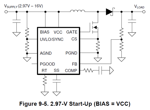
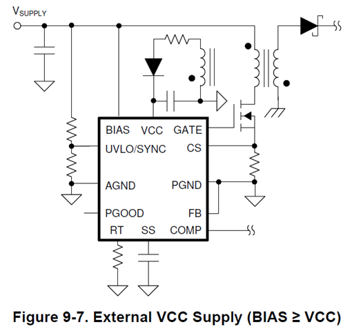
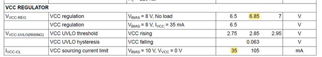
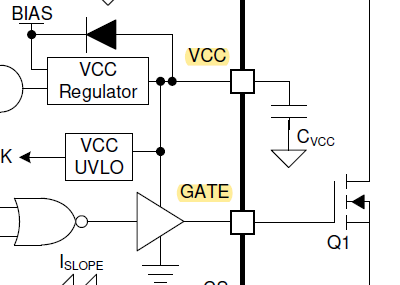
 i saw the VCC pin function from datasheet--"Output of the internal VCC regulator and supply voltage input of the MOSFET driver. Connect a
ceramic bypass capacitor from this pin to PGND.".

from the LM51551 block diagram, it seems like VCC only supply to pre-driver of GATE.

i have some questions about this architecture.

Q1: if bias is connected to a high voltage, then VCC regulator(LDO) will withstand large voltage. what about the efficiency of VCC regulator?

  • Hi Jay,

    Thanks for using the e2e forum.
    If BIAS voltage is very high, it is true that losses increase on the LDO as the VCC voltage is regulated to a fixed value.
    In such cases, it is possible to supply the VCC voltage externally as well to reduce these losses.
    Here it is important not to violate the abs max values of the pin.
    Also please note that LM5155 has an internal ESD diode from VCC to BIAS, so if  Vvcc > Vbias at any time, the device may take damage as the ESD diode is forward biased and may break very quickly.

    Best regards,
    Niklas

  • hi Niklas

    how to understand the following words? do you mean we can provide a voltage source to supply to VCC pin? 

    it is possible to supply the VCC voltage externally as well to reduce these losses.

    like the following pictures? these circuit can reduce the LDO regulator losses?

    how to calculate the LDO regulator losses?

    if Bisa=40v, Vcc=6.85v, LDO regulator losses is (40V-6.85V)*35mA=1.16W? is it right?  it looks too much!

  • Hi Jay,

    The first reference (figure 9-5) is not specifically focused on LDO loss reduction. At lower Vin (Vin 7V-15V), the losses are rather small.
    The second reference (figure 9-7) is the approach I meant. In flyback applications with high Vin (e.g. >30V), the VCC pin is often supplied by an aux winding of the transformer to avoid the LDO losses.

    The formula for calculating the LDO losses is not fully correct.
    The current value comes from the supply of the internal logic (see shutdown current) and from the current supplying the gate drivers.
    The gate driver current only flows when the gate capacitance of the FET is charged up, which only takes a few nanoseconds at the start of every switching cycle.
    So the final power loss depends on the selected FET and switching frequency.

    Best regards,
    Niklas 

  • hi Niklas

    The second reference (figure 9-7) is the approach I meant. In flyback applications with high Vin (e.g. >30V), the VCC pin is often supplied by an aux winding of the transformer to avoid the LDO losses.

    because customers are using SEPIC, so AUX winding approach may be different from flyback topology.

    The gate driver current only flows when the gate capacitance of the FET is charged up, which only takes a few nanoseconds at the start of every switching cycle.

    i think i got your point! this internal LDO regulator doesn't always work !